SENSOR USER GUIDE
REVISION HISTORY
| Revision No. | Description |
Date |
|---|---|---|
| 1.0 | 07/10/2025 |
1. OVERVIEW
This article takes the Comake_Pi_D1 development board with PCUPID series chips as an example to provide a reference for the use of image sensors. To use it, you need to understand some basic technical knowledge, including the CSI interface and CCI interface in the MIPI protocol, as well as the specifications of the sensor.
To ensure the image sensor outputs images normally, please follow these steps:
-
Confirm whether the hardware connection between the sensor and the SOC chip is correct
-
Clarify which pins on the SOC chip can be used for the MIPI interface of the sensor
-
Correctly configure the CSI and sensor_if interface parameters in the device tree (dts)
-
Confirm the module ko files that need to be loaded
-
Confirm the sensor driver ko files that need to be loaded
-
Correctly use the API interface of the MI module
2. KEYWORD
-
sensor : In embedded audio and video development, when referring to 'sensor' alone, it specifically denotes a CMOS image sensor, which is used for capturing image data.
-
sensor pad : Sensor hardware Jack location
-
mipi : It refers to the MIPI protocol suite, which includes protocols for touch, image capture, image display, etc.When MIPI is mentioned in the context of sensor usage, it refers to the CSI-2 protocol/interface (an image capture protocol).When MIPI is mentioned in the context of panel/display usage, it refers to the DSI protocol/interface (an image display protocol).
-
lane : In embedded system design, the term "lane" refers to an abstract concept derived from physical wiring, which includes:Clock Lane: Carries clock signals.Data Lane: Transmits data signals.Each lane may consist of one or more physical wires. For example, in the MIPI CSI-2 D-PHY (a physical layer protocol in the MIPI suite):Each data lane comprises two differential pairs: data- (negative) and data+ (positive).A sensor (e.g., GC2053) may utilize multiple data lanes. For instance, GC2053 uses 2 lanes, resulting in 4 physical data wires (2 pairs).By default, "lane" typically refers to a data lane unless explicitly specified otherwise.
3. FUNCTIONAL DESCRIPTION
The pcupid series chips support the sensor's MIPI mode, BT601 mode, and BT656 mode. Different modes are specified via DTS files. This chapter takes the sensor's MIPI mode as an example to explain the usage method of the sensor.
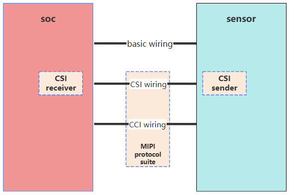
Description of Wiring Between Sensor and SoC
The wiring logic between the sensor and SoC mainly includes the following two parts:
-
Basic Wiring
The sensor itself needs to be connected to basic pins, such as the reset pin and clk (clock) input pin. These pins/wirings do not belong to the MIPI protocol suite.
-
MIPI Interface Wiring
The sensor is equipped with a MIPI interface (in some scenarios, the concepts of interface and protocol can be used interchangeably, and there is a situation where the two terms are mixed), including the following two types of interfaces:
-
CSI interface: Serves as the data plane interface of the sensor and is used to transmit image data
-
CCI interface: Serves as the control plane interface of the sensor and is used to configure the working mode and parameters of the sensor by reading and writing registers
-
Note: The CCI interface of the SigmaStar chip is implemented based on the I2C protocol.
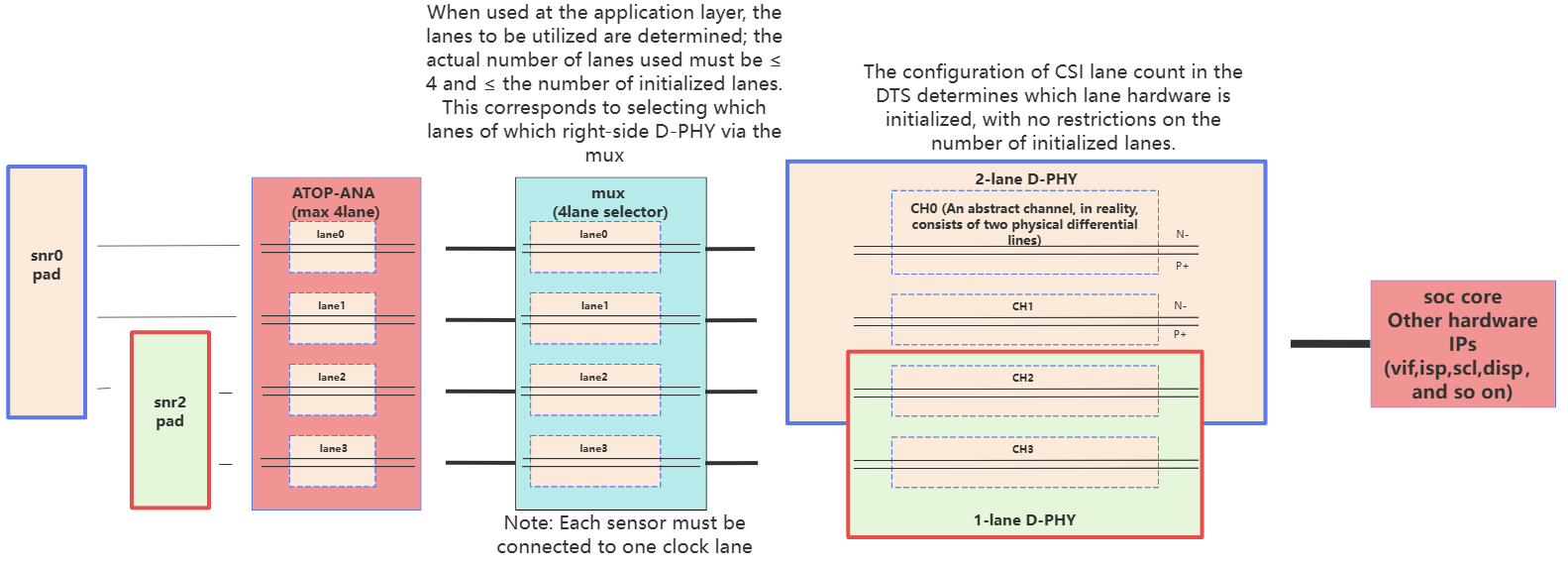
The CSI-2 interface RX receiver of the MIPI protocol suite inside the SoC chip hardware supports 2 data lanes and 2 clock lanes, and its configuration methods are as follows:
-
It can be configured as "1 clock lane + 2 data lanes" for a single sensor
-
It can also be configured as two groups of "1 clock lane + 1 data lane" to support two sensors simultaneously
For specific configuration details, please refer to the chip data sheet.
Description of Sensor Channel Allocation
-
snr0 corresponds to 3 lanes, including 2 data lanes and 1 clock lane
-
snr2 corresponds to 2 lanes, including 1 data lane and 1 clock lane
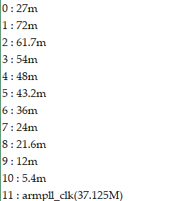
Different SigmaStar chips vary in their supported MCLK frequencies; the MCLK frequencies supported by the pcupid series chips are as follows
4. HARDWARE CONNECTION OVERVIEW
4.1 SoC hardware interface confirmation
Description of Configuration for Connection Between Sensor and SoC Pins
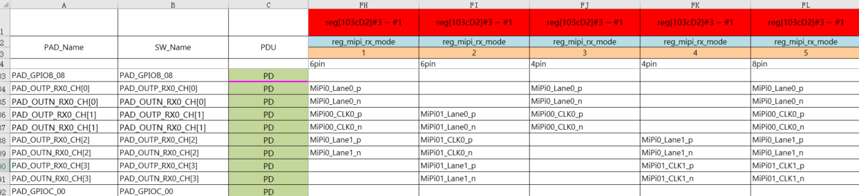
The following figures show the 'ARMTmux' sub-table of the hw_checklist for the on-board SoC chip of the Comake_Pi_D1 board. Writing different values to the reg_mipi_rx_mode register will result in different connections of the MIPI_RX pins to the sensor. It supports 2-lane independent streaming for SNR0, and simultaneous streaming with 1 lane for SNR0 plus 1 lane for SNR2. In the DTS, the snr_sr0_mipi_mode and snr_sr2_mipi_mode configuration items are used to pass values to the reg_mipi_rx_mode register.
Writing different values to the reg_sr00_mclk_mode and reg_sr01_mclk_mode registers will result in different configurations of the SoC's external sensor MCLK pins. Similarly, writing different values to the reg_sr00_rst_mode and reg_sr01_rst_mode registers will lead to different configurations of the SoC's external sensor RST pins. In the DTS, the snr_sr0_mipi_mclk_mode configuration item is used to pass values to the reg_sr00_mclk_mode register, and the snr_sr0_mipi_rst_mode configuration item is used to pass values to the reg_sr00_rst_mode register.
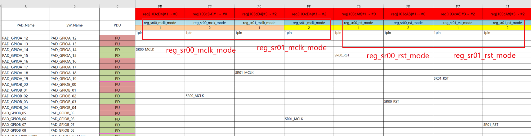
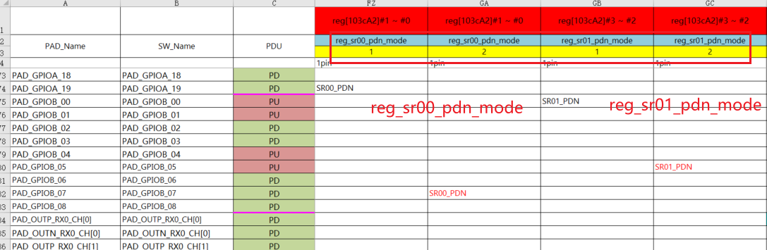
Writing different values to the reg_sr00_pdn_mode and reg_sr01_pdn_mode registers will result in different configurations of the SoC's external sensor PDN pins. In the DTS, the snr_sr0_mipi_pdn_mode configuration item is used to pass values to the reg_sr00_pdn_mode register. It should be noted that some sensor PDN pins can be left unconnected (floating) and do not require control. The PDN pin of SNR2 on the Comake_Pi_D1 board is floating and not connected to the SoC.
When configuring the reg_mipi_rx_mode registers of SNR0 and SNR2 to different values, there are different usage scenarios. The following are recommended usage combinations.
| type | One sensor streams independently with 2 lanes | Two sensors stream simultaneously with 1 lane each (1 lane + 1 lane) |
|---|---|---|
| mipi_rx_mode | set snr0 mode=1 | set snr0 mode=5 && snr2 mode=5 |
| mclk_mode | set snr0 mode=2 | set snr0 mode=2 && snr2 mode=2 |
| rst_mode | set snr0 mode=2 | set snr0 mode=2 && snr2 mode=2 |
| i2c_mode | set snr0 mode=4 | set snr0 mode=4 && snr2 mode=4 |
Note: The maximum specification of PCUPID supports 2 data lanes, which can be configured as either SNR0 with 2 lanes or split into SNR0 with 1 lane plus SNR2 with 1 lane.
Confirm which two terminal blocks SNR0 and SNR2 are connected to
On the Comake_Pi_D1 board, the pads of these two sensors are connected to the terminal blocks, making it convenient for developers to connect the sensors.
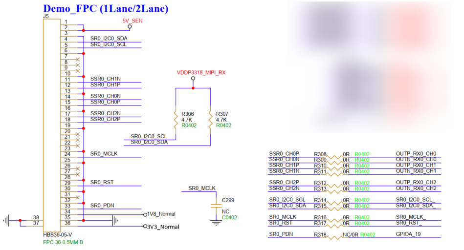
SNR0 is connected to the J5 terminal block. On the schematic diagram, 'OUTP_RX_CH0' and 'PAD_OUTP_RX0_CH[0]' are connected. On the J5 terminal block, the two pins SSR0_CH1N/P correspond to the data0 lane, SSR0_CH2N/P correspond to the data1 lane, and SSR0_CH0N/P correspond to the clk lane. It can be seen that this is a MIPI CSI-2 RX interface that supports a maximum of 2 data lanes.
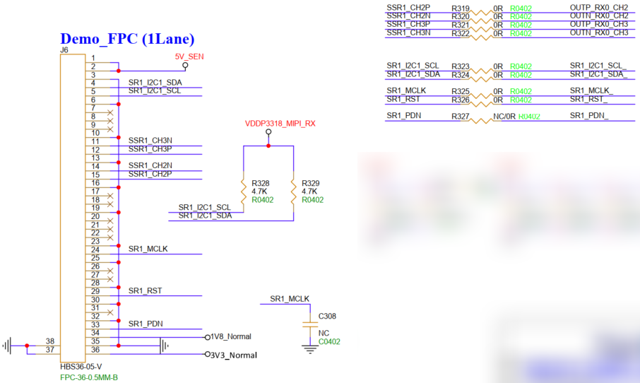
SNR2 is connected to the J6 terminal block. On the schematic diagram, 'OUTP_RX_CH2' and 'PAD_OUTP_RX0_CH[2]' are connected. On the J6 terminal block, the two pins SSR0_CH2N/P correspond to the data0 lane, and SSR0_CH3N/P correspond to the clk lane. It can be seen that this is a MIPI CSI-2 RX interface that supports a maximum of 1 data lane.
4.2 Sensor interface confirmation
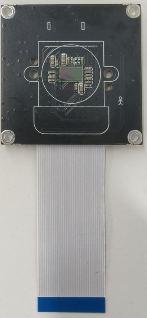
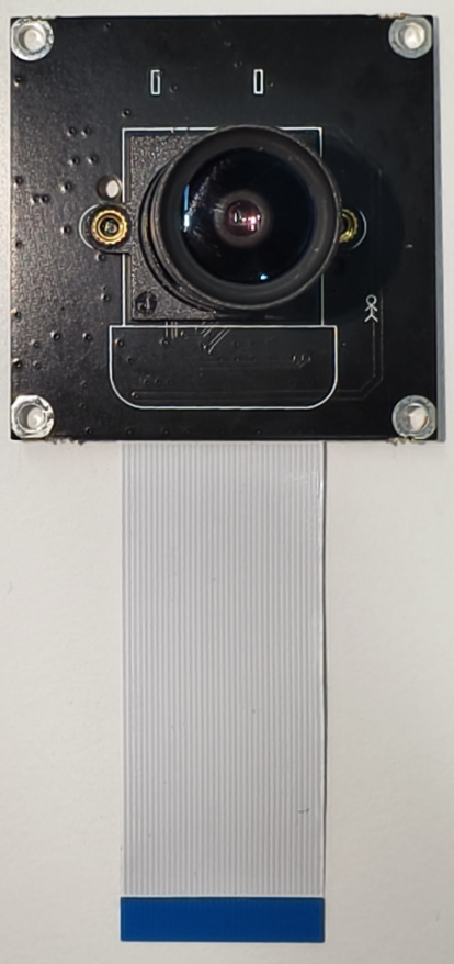
Confirm the sensor's terminal block. The Comake_Pi_D1 board is paired with the GC2053 sensor, which is not directly soldered onto the board but instead integrated into a separate sensor hardware module (a small hardware board). This sensor module connects to the Comake_Pi_D1 board via a flat cable.
Refer to the GC2053 data sheet. There are three categories of wires to be led out: one is the 'basic wiring' mentioned earlier, including RESET and MCLK; another is the 'CCI interface wires', including SBCL and SBDA; the third is the 'CSI interface wires', including MDN/P<0>, MDN/P<1>, and MCN/P.
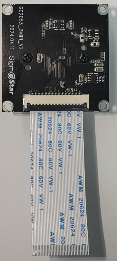
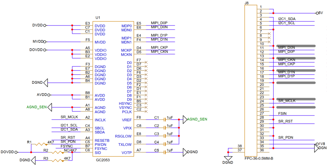
The schematic diagram of the GC2053 MIPI interface board is as follows. J8 on the right side is a terminal block; video streaming can be achieved by connecting one end of a flat cable to J8 and the other end to J5 or J6 on the Comake_Pi_D1 board. It can be seen that the pinout of the J8 terminal block matches that of J5 and J6.
4.3 MIPI interface pinout matching
To facilitate subsequent DTS configuration, the MIPI CSI wiring relationships are summarized here: the matching relationships between the J8 terminal block of the GC2053 MIPI interface board, the J5 and J6 terminal blocks of the Comake_Pi_D1 board, and the sensor pads.
When J8 is connected to J5 via a flat cable, the sensor and SNR0 pad are connected.
| J8 | J5 | snr0 pad |
|---|---|---|
| MIPI_D0N/P(data0 lane) | SSR0_CH1N/P | PAD_OUTN/P_RX0_CH[1] |
| MIPI_D1N/P(data1 lane) | SSR0_CH2N/P | PAD_OUTN/P_RX0_CH[2] |
| clock lane | SSR0_CH0N/P | PAD_OUTN/P_RX0_CH[0] |
If PAD_OUTN/P_RX0_CH[0] is abbreviated as CH0, the following table applies
| sensor | snr0 pad |
|---|---|
| data0 lane | CH1 |
| data1 lane | CH2 |
| clock lane | CH0 |
When J8 is connected to J6 via a flat cable, the sensor and SNR1 pad are connected. Following the same steps, the following table is obtained
| sensor | snr1 pad |
|---|---|
| data0 lane | CH3 |
| clock lane | CH2 |
Note: J5 and J6 share the CH2 pad, which imposes restrictions on the simultaneous use of the two sensors. This will be discussed in the DTS chapter.
5. KERNEL USAGE GUIDE
5.1 DTS configuration
As mentioned earlier, there are three categories of connections between the sensor and the SoC chip: 'basic wiring', 'CCI interface wiring', and 'CSI interface wiring'. These need to be properly configured in the DTS, and the kernel will initialize these three types of pads on the SoC based on the DTS configuration. The 'basic wiring' and 'CCI interface wiring' are configured via the sensorif node, while the 'CSI interface wiring' is configured via the CSI interface. The DTS configuration only determines which lanes of which SNR pads to initialize, with no quantity restrictions. The general configuration for the Comake_Pi_D1 board is as follows
Initialize 2 lanes of SNR0 and 1 lane of SNR2:
    csi: csi {
        compatible = "sstar,csi";
        io_phy_addr = <0x1f000000>;
        banks = <0x153C>,<0x153D>,<0x153E>,<0x1538>,<0x153A>,<0x153B>;
        atop_banks = <0x153F>;
        clkgen_banks = <0x1038>;
        interrupts=  <GIC_SPI INT_IRQ_MIPI_CSI2 IRQ_TYPE_LEVEL_HIGH>;
        status = "okay";
        /* Config max lane number */
        csi_sr0_lane_num = <2>;
        csi_sr2_lane_num = <1>;
        /* Config lane selection */
        csi_sr0_lane_select = <0 1 2>;
        csi_sr2_lane_select = <0 1>;
        /* Config lane P/N swap */
        csi_sr0_lane_pn_swap = <0 0 0>;
        csi_sr2_lane_pn_swap = <0 0>;
    };

    sensorif: sensorif {
        compatible = "sstar,sensorif";
        status = "okay";
        clocks = <&CLK_sr00_mclk>, <&CLK_sr01_mclk>;

        /* Config sensor 0 pad mux */
        snr_sr0_mipi_mode         = <5>;
        snr_sr0_mipi_rst_mode     = <2>;
        snr_sr0_mipi_pdn_mode     = <0>;
        snr_sr0_mipi_mclk_mode    = <2>;
        snr_sr0_rst_gpio          = <73>;
        snr_sr0_pdn_gpio          = <77>;

        ...

        /* Config sensor 2 pad mux */
        snr_sr2_mipi_mode         = <5>;
        snr_sr2_rst_gpio          = <77>;
        snr_sr2_mipi_pdn_mode     = <0>;
        snr_sr2_mipi_mclk_mode    = <2>;

        /* Config mclk 37.125MHz supported */
        snr_sr0_mclk_37p125 = <1>;
        snr_sr2_mclk_37p125 = <1>;

        /* Config CCI interface */
        snr0_mipi_i2c = <0>;
        snr2_mipi_i2c = <1>;
    };
The CSI section is explained as follows:
| parameter | explanation | note |
|---|---|---|
| interrupts | mipi rx csi interrupt | no modification required |
| clocks | mipi rx csi clock source | no modification required |
| csi_sr0_lane_num | configure the initialization count of SNR0 data lanes | Initialize as needed. SNR0 has a maximum of two data lanes, with optional values 0, 1, and 2. Note: The lane_num here must be less than or equal to the number of lanes specified by the reg_mipi_mode register. If SNR0 is initialized as 2 lanes, only 1 lane can be used in actual operation. |
| csi_sr0_lane_select | Configure the relative pinout order of SNR0 lanes for the CSI interface | <relative index of clk_lane, relative index of data0_lane, relative index of data1_lane> The relative indices are determined by comparing the CH values of clk_lane, data0_lane, and data1_lane. The smallest CH value corresponds to relative index 0, the middle one to 1, and the largest to 2. For example, when csi_sr0_lane_num=2, combined with the previously mentioned J8-J5-snr0 pinout order table, if clk_lane is connected to CH0, data0_lane to CH1, and data1_lane to CH2, then csi_sr0_lane_select=<0 1 2> |
| csi_sr0_lane_pn_swap | Configure whether the lane polarity of SNR0 is inverted | <polarity inversion flag of clk_lane, polarity inversion flag of data0_lane, polarity inversion flag of data1_lane> There are only two inversion flag values: 0 and 1. A value of 0 indicates no polarity inversion of the lane, with the N line connected to the N line and the P line connected to the P line. A value of 1 indicates polarity inversion of the lane, with the N line connected to the P line and the P line connected to the N line. This is a chip compatibility design to prevent revision caused by errors in external circuit design; simply modify the configuration here. All lanes of SNR0 and SNR2 on the Comake_Pi_D1 board have no polarity inversion. For example, csi_sr0_lane_pn_swap=<0 0 0> |
| csi_sr2_lane_num | Configure the initialization count of SNR2 data lanes | Initialize as needed. SNR2 has a maximum of 1 data lane, with optional values 0 and 1. |
| csi_sr2_lane_select | Configure the relative pinout order of SNR2 lanes for the CSI interface | Following the same analysis: clk_lane is connected to CH2, data0_lane to CH3. Since the CH value of clk_lane is 2 and that of data0_lane is 3, and 2 is less than 3, the relative index of clk_lane is 0 and that of data0_lane is 1. That is, csi_sr2_lane_select=<0 1> |
| csi_sr2_lane_pn_swap | Configure whether the lane polarity of SNR2 is inverted | Following the same analysis, there is no polarity inversion. For example, csi_sr2_lane_pn_swap=<0 0> |
Note: The default settings are snr0_lane_num=2 and snr2_lane_num=1. If only SNR0 is connected to a sensor, the sensor can output streams using 1 lane or 2 lanes. If only SNR2 is connected to a sensor, the sensor can only output streams using 1 lane. If both SNR0 and SNR2 are connected to sensors, attention must be paid to the CH2 lane sharing issue; for both sensors to output streams simultaneously, each must use only 1 lane.
The sensorif section is explained as follows:
| parameter | explanation | note |
|---|---|---|
| clocks | sensor mclk clock source | Configuration must follow the order of SNR0 and SNR2 |
| snr_sr0_mipi_mode | For the MIPI mode of SNR0, different modes primarily differ in the pads of the CSI interface | Refer to the ARMTmux sub-table in the hw_checklist |
| snr_sr0_mipi_rst_mode | For the mode of the reset pin when SNR0 uses the MIPI interface, different modes primarily differ in pads | Refer to the ARMTmux sub-table in the hw_checklist |
| snr_sr0_mipi_pdn_mode | For the mode of the PDN pin when SNR0 uses the MIPI interface, different modes primarily differ in pads | Refer to the ARMTmux sub-table in the hw_checklist |
| snr_sr0_mipi_mclk_mode | For the mode of the MCLK pin when SNR0 uses the MIPI interface, different modes primarily differ in terms of pads | Refer to the ARMTmux sub-table in the hw_checklist |
| snr_sr0_rst_gpio | The reset GPIO pin of SNR0 index | If both the reset mode and reset GPIO are configured, the GPIO setting takes precedence |
| snr_sr0_pdn_gpio | Settings for the PDN GPIO pin of SNR0 | If both PDN mode and PDN GPIO are configured, the GPIO setting takes precedence |
| snr_sr0_mclk_37p125 | Configure SNR0 to support 37.125 MHz | 1 - support 37.125MHz |
| snr0_mipi_i2c | Configure the I2C bus ID used by SNR0 | Configuration must be performed according to the actually used I2C bus |
5.2 padmux configures
The configurations of snr0_mipi_i2c and snr2_mipi_i2c shown in the previous section specify which I2C bus controller is used. The pins corresponding to the I2C controller must be designated via padmux, located in kernel/arch/arm/boot/dts/pcupid-comake-pi-d1-dual-sensor-padmux.dtsi
/ # cat kernel/arch/arm/boot/dts/pcupid-comake-pi-d1-dual-sensor-padmux.dtsi
...
//sensor 0/1 i2c
<PAD_GPIOB_00            PINMUX_FOR_I2C0_MODE_4           MDRV_PUSE_I2C0_SCL>,
<PAD_GPIOB_01            PINMUX_FOR_I2C0_MODE_4           MDRV_PUSE_I2C0_SDA>,
<PAD_GPIOB_04            PINMUX_FOR_I2C1_MODE_4           MDRV_PUSE_I2C1_SCL>,
<PAD_GPIOB_05            PINMUX_FOR_I2C1_MODE_4           MDRV_PUSE_I2C1_SDA>,
...
5.3 Project config configuration
Execute the "make menuconfig" command in the project directory, and then open, close or modify certain configuration items. If you want to save the modified configuration, you need to execute the "make savedefconfig" command, and then execute the "cp defconfig target defconfig" command
5.3.1 Configuring the packaged sensor driver ko
- CONFIG_SENSOR_LIST: Fill in the list of packaged sensor driver ko names, separate different ko names with spaces. This configuration item corresponds to the "List of sensor ko for image packaging" seen in make menuconfig
For example, a defconfig package by default includes imx323.ko, imx307_mipi.ko, and gc2053_mipi.ko files.
/project# make menuconfig
    Sensor  --->
        ...
        (imx323.ko imx307_mipi.ko gc2053_mipi.ko) List of sensor ko for image packaging  --->
        ...
5.3.2 Configuring the driver ko loaded by the sensor
-
CONFIG_SENSOR0 / 1 / 2: Fill in the driver ko name to be loaded by the snr interface. This configuration item corresponds to the "Snr0 / 1 / 2 ko" seen in make menuconfig
-
CONFIG_SENSOR0 / 1 / 2_OPT: Fill in the chmap parameter to be passed to the driver ko. This configuration item corresponds to the "Parameters for snr0 / 1 / 2 ko" seen in make menuconfig
The value of the parameter "chmap" determines the initialization of sensors of different interfaces
Initialize the sensor of snr0 interface separately ----> chmap=1
Initialize the sensor of snr2 interface separately ----> chmap=4
Initialize the sensors of snr0+snr2 interfaces at the same time ----> chmap=5
For example, the configuration of snr0 connected to gc2053 sensor alone is as follows:
/project# make menuconfig
    Sensor  --->
        (common/base_iqfile.bin) IQFILE_BASE_IQ0  --->
        () IQFILE_BASE_IQ1  --->
        () IQFILE_BASE_IQ2  --->
        () IQFILE_BASE_IQ3  --->
        (gc2053/gc2053_api.bin) IQFILE_API_IQ0  --->
        () IQFILE_API_IQ1  --->
        () IQFILE_API_IQ2  --->
        () IQFILE_API_IQ3  --->
        (gc2053_mipi.ko) List of sensor ko for image packaging  --->
        (gc2053_mipi.ko) Snr0 ko  --->
        (chmap=1) Parameters for snr0 ko  --->
        () Snr1 ko  --->
        () Parameters for snr1 ko  --->
        () Snr2 ko  --->
        () Parameters for snr2 ko  --->
    ...
For example, the configuration of snr0 connected to gc2053 sensor and snr2 connected to ov2710 sensor is as follows:
/project# make menuconfig
    Sensor  --->
        (common/base_iqfile.bin) IQFILE_BASE_IQ0  --->
        () IQFILE_BASE_IQ1  --->
        (common/base_iqfile.bin) IQFILE_BASE_IQ2  --->
        () IQFILE_BASE_IQ3  --->
        (gc2053/gc2053_api.bin) IQFILE_API_IQ0  --->
        () IQFILE_API_IQ1  --->
        (ov2701/ov2701_api.bin) IQFILE_API_IQ2  --->
        () IQFILE_API_IQ3  --->
        (gc2053_mipi.ko ov2701_mipi.ko) List of sensor ko for image packaging  --->
        (gc2053_mipi.ko) Snr0 ko  --->
        (chmap=1) Parameters for snr0 ko  --->
        () Snr1 ko  --->
        () Parameters for snr1 ko  --->
        (ov2701_mipi.ko) Snr2 ko  --->
        (chmap=4) Parameters for snr2 ko  --->
    ...
5.3.3 Configuring IQ Files
IQ files are parameter configuration files that the ISP module relies on. The IQ files of the PCUPID series chip boards are divided into the following two categories:
-
IQ file used by the driver layer : Basic fixed iq file (bin type, hereinafter referred to as "iq base bin file").
-
IQ file used by the application layer : IQ file modified as needed (bin type, hereinafter referred to as "IQ API bin file").
IQ file packaging instructions :
-
CONFIG_IQFILE_IQ0 / 1 / 2 / 3: Fill in the relative directory/file name of the iq base bin file to be packaged. The relative directory is relative to the path of "project/board/pcupid/iqfile/". This configuration item corresponds to IQFILE_BASE_IQ0 / 1 / 2 / 3 seen in make menuconfig.
-
CONFIG_IQAPI_IQ0 / 1 / 2 / 3: Fill in the "relative directory/file name" of the iq api bin file to be packaged. The relative directory is relative to the path of "project/board/pcupid/iqfile/". This configuration item corresponds to IQFILE_API_IQ0 / 1 / 2 / 3 seen in make menuconfig
For example, snr0 is connected to the gc2053 sensor, and the packaging configuration of the two IQ files is as follows:
/project# make menuconfig
    Sensor  --->
        (common/base_iqfile.bin) IQFILE_BASE_IQ0  --->
        () IQFILE_BASE_IQ1  --->
        () IQFILE_BASE_IQ2  --->
        () IQFILE_BASE_IQ3  --->
        (gc2053/gc2053_api.bin) IQFILE_API_IQ0  --->
        () IQFILE_API_IQ1  --->
        () IQFILE_API_IQ2  --->
        () IQFILE_API_IQ3  --->
    ...
Note: Some defconfigs will package all snr interface IQ files into the image by default. This has no effect on the normal use of the actual sensor. You can delete unused IQ files as needed.
These two bin files are performed in miservice.mk and customer.mk respectively (when the script reads and writes the configuration item value, the CONFIG_ prefix of the configuration item name needs to be deleted)
- Packaging of iq base bin: The iq base bin file specified by CONFIG_IQFILE_IQx is copied to the /config/iqfile/ directory in customer.mk and named iqfile0 / 1 / 2 / 3.bin
/ # cat project/image/packaging/common/miservice.mk
...
    if [ "$(IQFILE_IQ0)" != "" ]; then \
        cp -rf $(PROJ_ROOT)/board/$(CHIP)/iqfile/$(IQFILE_IQ0) $(miservice$(RESOURCE))/iqfile/ -vf; \
        cd $(miservice$(RESOURCE))/iqfile; \
        chmod +x $(shell echo $(IQFILE_IQ0) | awk -F'/' '{print $$NF}'); \
        ln -sf $(shell echo $(IQFILE_IQ0) | awk -F'/' '{print $$NF}') iqfile0.bin; cd -; \
    fi;
...
Note: mi_common.ko is fixed to load the IQ base bin file named iqfile0 / 1 / 2 / 3.bin. The packaged file name cannot be modified, but the packaged target path can be adjusted. After the package path is modified, the modparam.json file must be modified synchronously. See the "IQ File Loading Instructions" section below.
- Packaging of iq api bin: The iq api bin file specified by CONFIG_IQAPI_IQx is copied to the /customer/ directory in customer.mk and renamed to iqApiBin0 / 1 / 2 / 3.bin
/ # cat project/image/packaging/common/customer.mk
...
    # pack iq api bin
    if [ "$(IQAPI_IQ0)" != "" ]; then \
        cp -rf $(PROJ_ROOT)/board/$(CHIP)/iqfile/$(IQAPI_IQ0) $(customer$(RESOURCE))/iqApiBin0.bin -vf; \
    fi;
...
Note: Both the packaged iq base bin file name and the packaged target path can be modified. After modification, the application must be modified synchronously. See the "IQ File Loading Instructions" section below.
The final packaging results are as follows:
/ # ls -l /config/iqfile/
total 188
...
-rwxr-xr-x    1 13280    1513         39274 Aug 29  2025 base_iqfile.bin
lrwxrwxrwx    1 13280    1513            15 Aug 29  2025 iqfile0.bin -> base_iqfile.bin
...
/ #
/ # ls -l /customer/
total 9798
...
-rw-r--r--    1 13280    1513         92124 Aug 29  2025 iqApiBin0.bin
...
IQ file loading instructions:
The packaging process of the two types of IQ files has been introduced above. The following describes their specific loading methods:
-
Loading of iq base bin: When loading mi_common.ko, the ko will load the iq base bin file from the "rootPath" path specified in modparam.json, and read and write registers according to the file content to complete ISP hardware initialization. "rootPath" depends on the package path of the iq base bin file, and the two must be consistent
For example, miservice.mk has packaged the iq base bin file into the /config/iqfile/ directory of the file system, and the value of "rootPath" is as follows
/ # cat /config/modparam.json
{
...
"E_MI_MODULE_ID_ISP" :
{
    "rootPath" : "/config/iqfile"
},
...
}
Note: The path specified by "rootPath" can be modified at will. Other notes are as follows
-
If there is no E_MI_MODULE_ID_ISP node in modparam.json, or there is no rootPath configuration item under this node, the iq base bin file is loaded from the /config/iqfile/ directory by default.
-
If the iq base bin file is not loaded successfully, an error message will be printed on the serial port, such as "[ ERR ]Failed to open IQ file /config/iqfile/iqfile0.bin.Invalid path!!!!!!!!!"
-
-
Loading the iq api bin: When initializing the sensor, the application layer needs to actively call the MI_ISP_ApiCmdLoadBinFile() function and use the package path and name of the iq api bin file to load the file.
For example, customer.mk has packaged the iq api bin file into the file system /customer/iqApiBin0.bin, and the function call is as follows
MI_ISP_ApiCmdLoadBinFile(isp_dev_id, isp_channel_id, "/ customer/iqApiBin0.bin", 0);
Note:
-
If the target path and name of the iq api bin file packaged by customer.mk are changed, the function input parameters must also be changed accordingly.
-
If the iq api bin file is not loaded successfully, an error message will be printed on the serial port, such as "[isp_cus3a_api.c][MI_ISP_ApiCmdLoadBinFile] File path does not exist. /customer/iqApiBin0.bin not found!".
-
If both iq base/api bin files are not loaded successfully, in addition to the error printing, the image screen will also turn yellow.
-
Source of IQ file:
The above mentioned the packaging and loading process of the two types of IQ files. The following describes how to generate and modify these two types of IQ files.
-
Source of the IQ Base Bin: Provided by SigmaStar, included in the SDK, content cannot be modified. The final IQ Base Bin file name is fixed as iqfile0 / 1 / 2 / 3.bin, name cannot be changed
-
Source of IQ API bin: The default IQ API bin file provided by SigmaStar, which is included in the SDK. Customers can use the IQ tool to modify the file content and name as needed according to the sensor and usage scenario. For instructions on using the IQ tool, please refer to "ISP API Tuning SOP" document.
5.3.4 Configuring the packaged mi module
The SigmaStar platform must rely on mi_common.ko, mi_sensor.ko and other ko modules when using sensors. For details of the mi module, see the Functional Module Development Guide.
The mi module ko required to use the sensor is as follows
| Type | Function |
|---|---|
| mi_common.ko | Provides basic environment, underlying interfaces, and other functions for sensor usage |
| mi_sys.ko | Provides basic environment, underlying interface and other functions for sensor usage |
| mi_sensor.ko | Provides unified function implementation and calling interface for sensor drivers. |
| mi_vif.ko | Device driver for binding and enabling video input channels, quickly building a pipeline for receiving video streams |
The default mi module configuration packaged by defconfig is as follows, modify as needed
/project# make menuconfig
[*] SDK Config  --- >
[*] Interface Compile Config --- >
[*] common
[*] sys
[*] sensor
[*] vif
...
5.4 Loading related ko
5.4.1 Loading mi module ko
/customer/demo.sh loads the mi module ko by default, which is generated by customer.mk and is started by the /etc/init.d/rcS startup script.
/ # cat /customer/demo.sh
...
#mi module
insmod /config/modules/6.1/mi_common.ko g_ModParamPath=/config/modparam.json
insmod /config/modules/6.1/mi_sys.ko
insmod /config/modules/6.1/mi_sensor.ko
insmod /config/modules/6.1/mi_vif.ko
...
5.4.2 Loading sensor driver ko
/customer/demo.sh loads sensor driver ko by default
/ # cat /customer/demo.sh
...
#mi sensor
insmod /config/modules/6.1/gc2053_mipi.ko chmap= 5
...
5.5 Application Layer Calls
The snr vif initialization function is as follows. For more detailed application layer sensor usage process, please refer to the demo code in the SDK.
MI_S32 ST_VifInit(ST_Stream_Attr_T *pStreamAttr)
{
    /************************************************
    Step1:  Init Sensor
    *************************************************/
    MI_SNR_PADInfo_t stSnrPadInfo;
    MI_SNR_PlaneInfo_t stSnrPlaneInfo;


    MI_SNR_PADID snrPadId = pStreamAttr->u32SnrId;
    MI_U32 u32ResCount = 0;

    memset(&stSnrPadInfo, 0x0, sizeof(MI_SNR_PADInfo_t));
    memset(&stSnrPlaneInfo, 0x0, sizeof(MI_SNR_PlaneInfo_t));

    ExecFunc(MI_SNR_SetPlaneMode(snrPadId, FALSE), DRM_SUCCESS);
    ExecFunc(MI_SNR_QueryResCount(snrPadId, &u32ResCount), DRM_SUCCESS);

    if(pStreamAttr->u32SnrChoiceRes > u32ResCount-1){
        printf("MI_SNR_QueryResCount :%d\n", u32ResCount);
        return -1;
    }

    ExecFunc(MI_SNR_SetRes(snrPadId, pStreamAttr->u32SnrChoiceRes), DRM_SUCCESS);
    ExecFunc(MI_SNR_Enable(snrPadId), DRM_SUCCESS);

    /************************************************
    Step2:  Init Vif
    *************************************************/
    MI_VIF_GROUP VifGroupId = 0;
    MI_VIF_DEV VifDevId = 0;
    MI_VIF_DEV VifChnId = pStreamAttr->VifChnId;
    MI_VIF_PORT VifPortId = pStreamAttr->VifPortId;
    MI_VIF_GroupAttr_t stVifGroupAttr;
    MI_VIF_DevAttr_t stVifDevAttr;
    MI_VIF_OutputPortAttr_t stVifPortAttr;

    get_vif_from_snrpad(snrPadId, &VifGroupId, &VifDevId);


    memset(&stVifGroupAttr, 0x0, sizeof(MI_VIF_GroupAttr_t));
    memset(&stVifDevAttr, 0x0, sizeof(MI_VIF_DevAttr_t));
    memset(&stVifPortAttr, 0x0, sizeof(MI_VIF_OutputPortAttr_t));

    ExecFunc(MI_SNR_GetPadInfo(snrPadId, &stSnrPadInfo), DRM_SUCCESS);
    ExecFunc(MI_SNR_GetPlaneInfo(snrPadId, 0, &stSnrPlaneInfo), DRM_SUCCESS);
    printf(
                "MI_SNR_GetPlaneInfo %d, outputsize(%d, %d, %d, %d)\n",
                snrPadId,stSnrPlaneInfo.stCapRect.u16X,stSnrPlaneInfo.stCapRect.u16Y,
                stSnrPlaneInfo.stCapRect.u16Width,stSnrPlaneInfo.stCapRect.u16Height);

    stVifGroupAttr.eIntfMode = E_MI_VIF_MODE_MIPI;
    stVifGroupAttr.eWorkMode = E_MI_VIF_WORK_MODE_1MULTIPLEX;
    stVifGroupAttr.eHDRType = E_MI_VIF_HDR_TYPE_OFF;
    if (stVifGroupAttr.eIntfMode == E_MI_VIF_MODE_BT656) {
        stVifGroupAttr.eClkEdge = (MI_VIF_ClkEdge_e)stSnrPadInfo.unIntfAttr.stBt656Attr.eClkEdge;
    } else {
        stVifGroupAttr.eClkEdge = E_MI_VIF_CLK_EDGE_DOUBLE;
    }

    ExecFunc(MI_VIF_CreateDevGroup(VifGroupId, &stVifGroupAttr), DRM_SUCCESS);
    stVifDevAttr.stInputRect.u16X = stSnrPlaneInfo.stCapRect.u16X;
    stVifDevAttr.stInputRect.u16Y = stSnrPlaneInfo.stCapRect.u16Y;
    stVifDevAttr.stInputRect.u16Width = stSnrPlaneInfo.stCapRect.u16Width;
    stVifDevAttr.stInputRect.u16Height = stSnrPlaneInfo.stCapRect.u16Height;
    if (stSnrPlaneInfo.eBayerId >= E_MI_SYS_PIXEL_BAYERID_MAX) {
        stVifDevAttr.eInputPixel = stSnrPlaneInfo.ePixel;
    } else {
        stVifDevAttr.eInputPixel = (MI_SYS_PixelFormat_e)RGB_BAYER_PIXEL(
                stSnrPlaneInfo.ePixPrecision, stSnrPlaneInfo.eBayerId);
    }
    ExecFunc(MI_VIF_SetDevAttr(VifDevId, &stVifDevAttr), DRM_SUCCESS);
    ExecFunc(MI_VIF_EnableDev(VifDevId), DRM_SUCCESS);
    stVifPortAttr.stCapRect.u16X = stSnrPlaneInfo.stCapRect.u16X;
    stVifPortAttr.stCapRect.u16Y = stSnrPlaneInfo.stCapRect.u16Y;
    stVifPortAttr.stCapRect.u16Width = stSnrPlaneInfo.stCapRect.u16Width;
    stVifPortAttr.stCapRect.u16Height = stSnrPlaneInfo.stCapRect.u16Height;
    stVifPortAttr.stDestSize.u16Width = stSnrPlaneInfo.stCapRect.u16Width;
    stVifPortAttr.stDestSize.u16Height = stSnrPlaneInfo.stCapRect.u16Height;
    stVifPortAttr.eFrameRate = E_MI_VIF_FRAMERATE_FULL;
    if (stSnrPlaneInfo.eBayerId >= E_MI_SYS_PIXEL_BAYERID_MAX) {
        stVifPortAttr.ePixFormat = stSnrPlaneInfo.ePixel;
    } else {
        stVifPortAttr.ePixFormat = (MI_SYS_PixelFormat_e)RGB_BAYER_PIXEL(
                stSnrPlaneInfo.ePixPrecision, stSnrPlaneInfo.eBayerId);
    }
    ExecFunc(MI_VIF_SetOutputPortAttr(VifDevId, VifPortId, &stVifPortAttr), DRM_SUCCESS);


    return 0;
}
5.6 Sensor Driver Development
5.6.1 Sensor Driver Development Reference
The sensor driver implementation for different interface types is basically the same. For details, please refer to Sensor_Porting
5.6.2 Introduction to sensor driver functions
| Parameter Name | Function |
|---|---|
| cus_camsensor_init_handle | Set basic sensor parameters and register function callback |
| handle->pCus_sensor_init handle->pCus_sensor_release |
Initialization Deinitialization sensor (configure parameters through iic) |
| handle->pCus_sensor_poweron handle->pCus_sensor_poweroff |
Power on\power off function (poweron will be called before sensor_init) |
| handle->sif_bus | Interface type (MIPI, DVP, etc.) |
| handle->data_prec | Data type (raw8\10\12 YUV, etc.) |
| handle->bayer_id handle->RGBIR_id |
BAYE or RGB arrangement order |
| handle->interface_attr.attr_mipi | MIPI configuration |
| handle->video_res_supported | How many configurations are supported |
| handle->i2c_cfg | iic configuration |
| handle->pwdn_POLARITY handle->reset_POLARITY handle->VSYNC_POLARITY handle->HSYNC_POLARITY handle->PCLK_POLARITY |
Control pin polarity configuration |
| handle->mclk | MCLK clk |
| sensor_if->SetCSI_Clk sensor_if->SetCSI_Lane sensor_if->SetCSI_LongPacketType |
CSI configuration (clk, number of lanes, supported packet types (1c means support for Raw8, 10, 12)) |
| Preview_line_period | Line length (including h blank) |
| params->expo.vts | Frame length (including V blank & h blank) |
PS: Preview_line_period = 1*10^9/(fps*(data_h+v_blank))

6. Verified Sensor List
6.1. MIPI Interface Camera Sensor Support list
During the chip verification phase, the verified MIPI interface sensors are shown in the following table:
| Interface Type | Lane Number | Kind | Key Indicator | Data Format |
|---|---|---|---|---|
| MIPI | 2Lane | IMX307 | 1920x1080@30FPS,2lane | Bayer |
| 2/1Lane | gc2053 | 1920x1080@30FPS,2/1lane | Bayer | |
| 1Lane | sc035hgs | 640x480@30FPS,1lane | Bayer |
6.2. BT601(DVP) Interface Camera Sensor Support List
During the chip verification phase, the verified sensors of the BT601(DVP) interface are shown in the following table:
| Interface Type | Data Pin Number | Kind | Key Indicator | Data Format | parallel | 10 pin | IMX323 | 1920x1080@30fps | Bayer |
|---|
6.3. BT656 Interface Camera Sensor Support List
During the chip verification phase, the verified BT656 interface sensors are shown in the following table:
| Interface Type | Data Pin Number | Kind | Key Indicator | Data Format |
|---|---|---|---|---|
| BT656 | 8pin | NVP6158C | 1280x720@30fps | YUV |
7. FAQ
Q1: How to check sensor output image
echo dumptaskfile 0 2 /mnt/pcm > /proc/mi_modules/mi_isp/mi_isp0 echo dumptaskfile 0 2 /mnt/pcm > /proc/mi_modules/mi_scl/mi_scl0
/mnt/pcm : image dump path 2: catch 2 frame 0: chnNum
Q2: How to confirm sensor interrupt info
please refer to MI VIF API 5.PROCFS INTRODUCTION