RISCV_SPI USER GUIDE
1. OVERVIEW
Serial Peripheral Interface (SPI), referred to as SPI, is a high-speed synchronous serial interface technology launched by Motorola. It is mainly used in EEPROM, Flash, real-time clock (RTC), analog-to-digital converter (ADC), digital signal processor (DSP) and other devices.
MSPI, or Master SPI device, is an IP provided by SigmaStar specifically for SPI communication master devices. It can communicate with various external SPI slave devices and meet the needs of most SPI communication protocol devices.
2. KEYWORD DESCRIPTION
-
MISO / SDO: Master input slave output. (data comes from the slave)
-
MOSI / SDI: Master output slave input. (data comes from the master)
-
SCLK / SCK: Serial clock signal, generated by the master and sent to the slave.
-
CS / SS: Slave Select chip select signal, sent by the master to control which slave to communicate with, usually a low-level valid signal.
-
CPOL / CKP: Clock polarity, indicating the high and low levels of the clock in the default state.
-
CPHA / CKE: Clock phase, indicating the specific phase of the clock signal when collecting data.
-
SPI Mode: The configuration of the SPI clock polarity and phase can output 4 SPI modes.
SPI Mode CPOL CPHA 0 [00] 0 0 1 [01] 0 1 2 [10] 1 0 3 [11] 1 1
3. Functional Description
-
MSPI (Master SPI) can only be used as a master device, not a slave device.
-
The hardware supports 2 groups of MSPI and Motorola SPI standard timing. The register bank of MSPI and the maximum software chip select supported are as follows:
MSPI Bus bank addr cs_num 0 1110H 2 1 1119H 2 -
Supports full-duplex read and write, half-duplex read and write in FIFO mode, and only supports half-duplex read and write in DMA mode.
-
Supports 4-wire communication (MISO + MOSI + SCLK + CS) and 3-wire communication. (MOSI + SCLK + CS)
-
8-byte read and write buffer (FIFO mode), byte transmission 1-bit to 16-bit configurable bit width.
-
Source Clock: 12M, 104M, 108M, 144M. The actual SPI communication frequency optional gear is 8 gears of each Source Clock division (the division coefficient is 2, 4, 8, 16, 32, 64, 128, 256), a total of 32 gears, so the SPI communication frequency range is 46875HZ~72MHz. The target frequency can be set by assigning the max_speed_hz variable in the struct mspi_setup structure; and the actual communication frequency will select the gear closest to the target frequency but less than the target frequency. Frequency gear table is as follows.
NO. SPI Clock Rate 1 46875 2 93750 3 187500 4 375000 5 421861 6 421875 7 562500 8 750000 9 843723 10 843750 11 1125000 12 1500000 13 1687446 14 1687500 15 2250000 16 3000000 17 3374892 18 3375000 19 4500000 20 6000000 21 6749785 22 6750000 23 9000000 24 13499571 25 13500000 26 18000000 27 26999143 28 27000000 29 36000000 30 53998287 31 54000000 32 72000000
4. HARDWARE CONNECTION INTRODUCTION
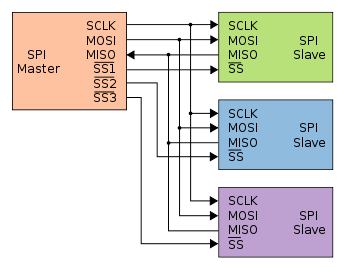
MSPI only supports one master and multiple slaves architecture. As the name implies, there can be only one master device and one or more slave devices on one bus. The slave selection signal line is often called the chip select signal line, also known as CS and SS, and is represented by SS below. When multiple SPI slave devices are connected to the SPI host, the other signal lines SCLK, MOSI and MISO of the device are connected in parallel to the same SPI bus at the same time, that is, no matter how many slave devices there are, they only use these three lines together; and each slave device has an independent SS signal line, which occupies a pin of the host, that is, there are as many chip select signal lines as there are slave devices. There is no device address in the SPI protocol. It uses the SS signal line for addressing. When the host wants to select a slave device, it sets the SS signal line of the slave device to a low level (the default is a low level), and the slave device is selected, that is, the chip select is valid, and then the host starts SPI communication with the selected slave device. Therefore, SPI communication starts with the SS line being set to a low level and ends with the SS line being pulled high.
5. RISCV USAGE INTRODUCTION
When communicating via MSPI, the following basic steps must be followed:
-
Hardware device connection;
-
Confirm whether CONFIG_MSPI_SUPPORT is enabled;
-
SYSDESC file configures requirement attributes;
-
PADMUX settings;
-
API calls to execute communication.
5.1. DRIVER PATH
sc/driver/sysdriver/mspi/drv/src/drv_mspi.c

sc/driver/sysdriver/mspi/hal/pcupid/src/hal_mspi.c

sc/driver/sysdriver/mspi/hal/pcupid/inc/hal_mspi.h

sc/driver/sysdriver/mspi/hal/pcupid/inc/hal_mspireg.h

sc/driver/sysdriver/mspi/hal/pcupid/inc/hal_mspi_cfg.h

sc/driver/sysdriver/mspi/os/mspi_os.h

sc/driver/sysdriver/mspi/drv/pub/drv_mspi.h

sc/driver/sysdriver/mspi/drv/src/drv_mspi_test.c
5.2. CONFIG Configuration
The config file is located at mak/options_chipname_riscv_isw.mak, enable CONFIG_MSPI_SUPPORT.
CONFIG_MSPI_SUPPORT = TRUE
5.3. SYSDESC Configuration
The chipname.sys file is located at sc/driver/sysdriver/sysdesc/hal/chipname/pub.
<mspi0>
    [reg_u32_u16] 0x2222000 0x200;
    [interrupts_u8] INT_IRQ_MSPI_0;
    [camclk_u16] CAMCLK_mspi0;
    [dma_u8] 1;
    [cs_num_u8] 2;
    [cs_ext_u32] PAD_UNKNOWN;
    [4to3_mode_u8] 0;
    [clk_out_mode_u32] 0;
    [padmux_u16] PINMUX_FOR_UNKNOWN_MODE, PINMUX_FOR_UNKNOWN_MODE;
    [status_u8] 1;
The attributes supported by the SPI master driver are as follows:
| Attribute | Description | Remark |
|---|---|---|
| reg_u32_u16 | Used to specify the IO address of the SPI register bank | No need to modify |
| interrupts_u8 | Used to specify the hardware interrupt number to be used | No need to modify |
| camclk_u16 | Used to specify the mspi clock | No need to modify |
| dma_u8 | Used to specify whether to enable DMA mode | Can be modified as needed |
| clk_out_mode_u32 | Used to specify whether to enable clk-out-mode | Can be modified as needed |
| cs_num_u8 | Used to specify the number of cs pads that come with the Engine | Used with cs-ext_u32 |
| cs_ext_u32 | Used to specify the pad index to be used in addition to the cs that comes with the Engine | Can be modified as needed |
| 4to3_mode_u8 | Used to specify whether to enable 4Wires as 3Wires | Can be modified as needed |
| padmux_u16 | Used to select the padmux of mspi | Can be modified as needed |
| status_u8 | Used to specify whether to enable mspi | Can be modified as needed |
5.3.1 DMA Mode
SigmaStar SPI Master supports two basic communication modes: fifo mode and dma mode. When the SPI Master is in fifo mode, the SPI Master driver writes the data to be sent into the SPI Master's send buffer and reads the received data from the receive buffer. The send buffer and receive buffer are registers in the SPI Master peripheral, and the capacity of the send buffer and receive buffer is 8 bytes each. Since the SPI Master works in fifo mode, the software needs to participate in the operation of the send buffer and receive buffer, so the waveform will be affected by software scheduling, and there will be a certain interval between each transmission.
When the SPI Master is in dma mode, the driver only needs to set the address of the data to be sent and the address where the received data needs to be stored to the SPI Master DMA-related registers, and the SPI Master will automatically send and receive data continuously. This process does not require software participation. Therefore, when the SPI Master works in dma mode, the SPI waveform continuity is better.
When the amount of data sent or received during the communication between the SPI Master and the SPI Device is small, you can consider using fifo mode, which has higher work efficiency. When the SPI Master and SPI Device communicate, the amount of data sent or received is large, such as receiving SPI Sensor data, etc. If fifo mode is used for such large-scale data communication, the system CPU usage will be very high, affecting system efficiency. In the scenario of large-scale data communication, dma mode can be considered.
[Note] Currently, SigmaStar SPI Master dma mode only supports half-duplex working mode, and the sending and receiving of SPI Master share the same dma channel. When the device needs to use full-duplex communication, only fifo mode can be used. The dma_u8 attribute specifies whether to use fifo mode or dma mode in half-duplex mode. When the Device driver needs to use full-duplex communication, the Master driver will automatically switch to fifo mode. When dma mode is turned on, full-duplex can be enabled through the transmission parameters, so if you want to use full-duplex mode, you can also specify the dma_u8 attribute.
5.3.2 cs-num
The maximum value of the hardware preset cs number, cs_num_u8 = n, the software chip select number is the MSPI chip select 0 ~ n-1; if you want to use the MSPI software chip select cs0, cs1, you need to configure cs_num_u8 = 2.
5.3.3 cs-ext
The function of adding additional cs pins implemented by the driver. When the hardware preset cs pins are not enough, you can configure additional cs pins in dtsi as an expansion. The cs_ext_u32 chip select number starts from the value of cs_num_u8. For example, if cs_ext_u32 = 2, the first cs-ext pin is cs2. The method to configure additional cs is to open the cs_ext_u32 property under the dtsi node and configure the pad id to be used as an expansion of cs. At the same time, it is recommended to configure the corresponding pad as GPIO MODE in xxx-padmux.dtsi. The following is to use PAD_I2C0_SCL as an expansion of cs:
<PAD_GPIOE_14           PINMUX_FOR_MSPI0_MODE_1       MDRV_PUSE_SPI0_CK>,
<PAD_GPIOE_16           PINMUX_FOR_MSPI0_MODE_1       MDRV_PUSE_SPI0_DI>,
<PAD_GPIOE_17           PINMUX_FOR_MSPI0_MODE_1       MDRV_PUSE_SPI0_DO>,
<PAD_GPIOE_15           PINMUX_FOR_MSPI0_MODE_1       MDRV_PUSE_SPI0_CZ>,
<PAD_I2C0_SCL           PINMUX_FOR_GPIO_MODE          MDRV_PUSE_SPI0_CZ2>,
5.3.4 clk-out-mode
clk-out-mode is a special mode supported by SigmaStar SPI Master. When SPI Master is in clk_out_mode_u32, MOSI and MISO of SPI Master no longer send or receive data according to the given data, and the Clock signal of SPI Master will continuously output square waves. The application scenario of this function is to use the clock output by SPI Master as the working clock of other devices. The value of clk_out_mode_u32 attribute is used to specify the frequency of the output clock. To configure clk_out_mode_u32, you only need to turn on the clk_out_mode_u32 attribute of that device in chipname.sys and configure the corresponding waveform frequency to be output:
[clk_out_mode_u32] 3750000; //Enable clk-out-mode, output the 3.75M frequency waveform
The selectable output frequency is the same as the normal operating frequency of MSPI, refer to the Frequency Range Table.
5.3.5 4 to 3 Mode
The SPI Master 3-wire mode of some platforms does not support dma mode. If you need 3-wire dma mode communication, you can enable 4 to 3 mode. In terms of hardware, short the MOSI and MISO of the Master and connect them to the SDAT of the Device, as shown below:
When the driver is reading data, MOSI will automatically switch to GPIO Input Mode so as not to interfere with the waveform input of MISO, thereby achieving the goal of using the 4-wire mode as the 3-wire mode. If you want to use this function, just turn on the 4to3-mode attribute in the dtsi node, that is:
[4to3_mode_u8] 1; //Enable 4to3-mode
Note: The pins of MSPI in 4to3 mode cannot be used as other modes. MISO in 3-wire mode can be used as other functions, provided that the mode has a higher priority than MSPI, such as gpio.
5.4. PADMUX Setting
CONFIG configuration: CONFIG_PADMUX_SUPPORT=TRUE
If the chipname_xxx.sys file is configured with the attribute <padmux>, then the PADMUX setting is directly configured here:
<padmux>
    [schematic_u32_u32_u32]
              PAD_GPIOE_14   PINMUX_FOR_MSPI0_MODE_1    MDRV_PUSE_SPI0_CZ,
              PAD_GPIOE_16   PINMUX_FOR_MSPI0_MODE_1    MDRV_PUSE_SPI0_CK,
              PAD_GPIOE_17   PINMUX_FOR_MSPI0_MODE_1    MDRV_PUSE_SPI0_DI,
              PAD_GPIOE_15   PINMUX_FOR_MSPI0_MODE_1    MDRV_PUSE_SPI0_DO,
    [status_u8] 1;
Otherwise, enable the PADMUX driver and configure the pin multiplexing function in the chipname-xxx-padmux.c file, which is located in sc/driver/sysdriver/padmux/hal/chipname/src. You only need to add the following content to the corresponding schematic attribute:
pad_info_t schematic[] =
{
    {PAD_GPIOE_14,    PINMUX_FOR_MSPI0_MODE_1,    MDRV_PUSE_SPI0_CZ},
    {PAD_GPIOE_16,    PINMUX_FOR_MSPI0_MODE_1,    MDRV_PUSE_SPI0_CK},
    {PAD_GPIOE_17,    PINMUX_FOR_MSPI0_MODE_1,    MDRV_PUSE_SPI0_DI},
    {PAD_GPIOE_15,    PINMUX_FOR_MSPI0_MODE_1,    MDRV_PUSE_SPI0_DO},
};
The first column is the pin index number, which can be queried in sc/drivers/sysdriver/gpio/hal/chipname/pub/gpio.h;
The second column is the mode definition, which can be queried in sc/drivers/sysdriver/gpio/hal/chipname/pub/padmux.h;
The third column is the index name of the pin and matching mode, which can be queried in sc/drivers/sysdriver/padmux/drv/pub/drv_puse.h.
MSPI0 hardware group padmux list
| MSPI Bus | Register addr | Padmod | Pad | Pin Name |
|---|---|---|---|---|
| 0 | bank 103CH offset 6CH bit[6:4] | 1 | MSPI0_CZ0 | PAD_GPIOE_15 |
| MSPI0_CK | PAD_GPIOE_14 | |||
| MSPI0_DI | PAD_GPIOE_16 | |||
| MSPI0_DO | PAD_GPIOE_17 | |||
| 2 | MSPI0_CZ0 | PAD_GPIOA_12 | ||
| MSPI0_CK | PAD_GPIOA_13 | |||
| MSPI0_DI | PAD_GPIOA_14 | |||
| MSPI0_DO | PAD_GPIOA_15 | |||
| 3 | MSPI0_CZ0 | PAD_GPIOC_07 | ||
| MSPI0_CK | PAD_GPIOC_06 | |||
| MSPI0_DI | PAD_GPIOC_04 | |||
| MSPI0_DO | PAD_GPIOC_05 | |||
| 4 | MSPI0_CZ0 | PAD_GPIOE_21 | ||
| MSPI0_CK | PAD_GPIOE_22 | |||
| MSPI0_DI | PAD_GPIOE_23 | |||
| MSPI0_DO | PAD_GPIOE_24 | |||
| bank 103CH offset 6CH bit[1:0] | mspi0 cz1 mode 1 | MSPI0_CZ1 | PAD_GPIOE_13 | |
| mspi0 cz1 mode 2 | MSPI0_CZ1 | PAD_EMMC_D7 |
5.5 Sample code
The demo source code is located in sc/driver/sysdriver/mspi/drv/src/drv_mspi_test.c
Usage examples:
static int spi_ut_test(CLI_t * cli, char * p)
{
    u32  i;
    s32  ret;
    u8   argc;
    u32  port;
    u32  cs_select;
    u32  speed;
    char *cmd;
    struct mspi_setup setup = {0};
    struct mspi_tfr transfers[2] = {0};

    argc = CliTokenCount(cli);

    if (argc != 4)
        return eCLI_PARSE_INPUT_ERROR;

    cmd = CliTokenPop(cli);

    if (CliTokenPopNum(cli, &port, 0) != eCLI_PARSE_OK)
    {
        return eCLI_PARSE_INPUT_ERROR;
    }

    if (CliTokenPopNum(cli, &cs_select, 0) != eCLI_PARSE_OK)
    {
        return eCLI_PARSE_INPUT_ERROR;
    }

    if (CliTokenPopNum(cli, &speed, 0) != eCLI_PARSE_OK)
    {
        return eCLI_PARSE_INPUT_ERROR;
    }

    setup.bus_num = (u8)port;
    setup.chip_select = (u8)cs_select;
    setup.max_speed_hz = speed;
    setup.mode &= ~(MSPI_SETUP_CPHA | MSPI_SETUP_CPOL);
    //mspi initial configure
    ret = drv_mspi_setup(&setup);
    if(ret)
    {
        cliPrintf("drv_mspi_setup fail : %d\n", ret);
        return eCLI_PARSE_UNKNOWN;
    }
    //read
    if (strcmp(cmd, "r") == 0)
    {
        wdata[0] = 0x03;
        wdata[1] = 0x00;
        wdata[2] = 0x00;
        wdata[3] = 0x00;
        transfers[0].tx_buf = wdata;
        transfers[0].rx_buf = NULL;
        transfers[0].len = 4;
        transfers[0].bits_per_word = 8;
        transfers[1].tx_buf = NULL;
        transfers[1].rx_buf = rdata;
        transfers[1].len = 256;
        transfers[1].bits_per_word = 8;
        ret = drv_mspi_transfer(&setup, transfers, 2);
        if (ret)
        {
            cliPrintf("drv_mspi_transfer fail : %d\n", ret);
            return eCLI_PARSE_UNKNOWN;
        }
    }
    //write
    else if (strcmp(cmd, "w") == 0)
    {
        wdata[0] = 0x06;
        transfers[0].tx_buf = wdata;
        transfers[0].rx_buf = NULL;
        transfers[0].len = 1;
        transfers[0].bits_per_word = 8;
        ret = drv_mspi_transfer(&setup, transfers, 1);
        if (ret)
        {
            cliPrintf("drv_mspi_transfer fail : %d\n", ret);
            return eCLI_PARSE_UNKNOWN;
        }

        wdata[0] = 0x02;
        wdata[1] = 0x00;
        wdata[2] = 0x00;
        wdata[3] = 0x00;
        for (i = 0; i < 256; i++)
        {
            wdata[i+4] = i;
        }
        transfers[0].tx_buf = wdata;
        transfers[0].rx_buf = NULL;
        transfers[0].len = 260;
        transfers[0].bits_per_word = 8;
        ret = drv_mspi_transfer(&setup, transfers, 1);
        if (ret)
        {
            cliPrintf("drv_mspi_transfer fail : %d\n", ret);
            return eCLI_PARSE_UNKNOWN;
        }
    }
    ...
    return eCLI_PARSE_OK;
}
When .rx_buff is not null and .tx_buff is null in struct mspi_tfr, MSPI Master performs half-duplex read operation; when .rx_buff is null and .tx_buff is not null, half-duplex write operation is performed; when .rx_buff and .tx_buff are not null, full-duplex read and write operation is performed even if dma mode is turned on. The corresponding waveform diagram is as follows:
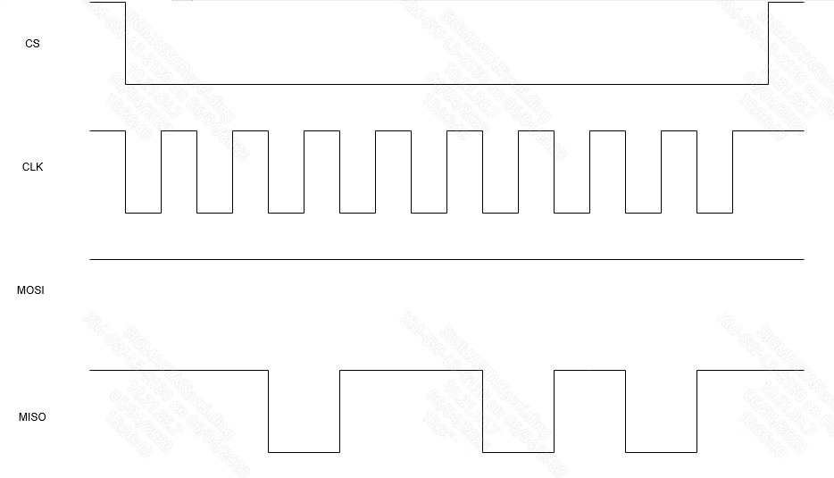
In the figure, MOSI corresponds to the data in .tx_buff, and MISO corresponds to the data in .rx_buff.
6. API Reference
-
The header file is located at
sc/driver/sysdriver/mspi/drv/pub/drv_mspi.hstruct mspi_setup { u8 bus_num; /* mspi bus number */ u32 max_speed_hz; /* transfer speed */ u8 chip_select; u32 mode; /* define below */ #define SPI_CPHA 0x01 /* clock phase */ #define SPI_CPOL 0x02 /* clock polarity */ #define SPI_MODE_0 (0|0) /* (original MicroWire) */ #define SPI_MODE_1 (0|SPI_CPHA) #define SPI_MODE_2 (SPI_CPOL|0) #define SPI_MODE_3 (SPI_CPOL|SPI_CPHA) #define SPI_CS_HIGH 0x04 /* chipselect active high? */ #define SPI_LSB_FIRST 0x08 /* per-word bits-on-wire */ #define SPI_3WIRE 0x10 /* SI/SO signals shared */ #define SPI_LOOP 0x20 /* loopback mode */ #define SPI_NO_CS 0x40 /* 1 dev/bus, no chipselect */ #define SPI_READY 0x80 /* slave pulls low to pause */ #define SPI_TX_DUAL 0x100 /* transmit with 2 wires */ #define SPI_TX_QUAD 0x200 /* transmit with 4 wires */ #define SPI_RX_DUAL 0x400 /* receive with 2 wires */ #define SPI_RX_QUAD 0x800 /* receive with 4 wires */ #define SPI_CS_WORD 0x1000 /* toggle cs after each word */ #define SPI_TX_OCTAL 0x2000 /* transmit with 8 wires */ #define SPI_RX_OCTAL 0x4000 /* receive with 8 wires */ #define SPI_3WIRE_HIZ 0x8000 /* high impedance turnaround */ }; -
This function module provides the following interfaces:
API name Function drv_mspi_setup Set properties including mode, frequency, chip select, etc. drv_mspi_transfer Data transmission.
6.1 drv_mspi_setup
-
Function
Set properties including mode, frequency, chip select, etc.
-
Syntax
int drv_mspi_setup(struct mspi_setup *setup)
-
Parameters
Parameter name Description setup struct mspi_setup describes the communication parameter configuration, the parameters include the bus number to be set, cs chip select number, communication frequency, mode, etc. -
Return value
Result Description Success Return 0 Failure Return non-zero value
6.2 drv_mspi_transfer
-
Function
Data Transfer
-
Syntax
int drv_mspi_transfer(struct mspi_setup *setup, struct mspi_tfr *tfr, u32 length)
-
Parameters
Parameter name Description setup mspi parameter configuration, the parameters include the bus number to be set, cs chip select number, communication frequency, mode, etc. tfr struct mspi_tfr is used to describe communication information, including communication data, bit width, etc. length The number of mspi_tfr -
Return value
Result Description Success Return 0 Failure Return non-zero value
7. FAQ
When communication anomalies occur, you can refer to the following aspects for problem debugging. Several common troubleshooting directions are provided. In addition, it is recommended to capture the waveform during the debugging process for easy analysis.
| Troubleshooting | Common Problems |
Notes |
|---|---|---|
| padmux | 1. No waveform, cannot be triggered | Check whether the register value has been set. For padmux settings, refer to the PADMUX section or the padmux module description |
| Is the linux dtsi configuration in conflict with riscv | It may cause mspi to fail to take effect under riscv | Turn off the linux dtsi configuration |
| Clock source | 1. LA captures data incorrectly; | This situation may occur when the clock rate is set too high, such as exceeding 45m. At this time, you can adjust the gpio drive capability |
| cs_ext | The extension pin function cannot be used | Please confirm whether it is an old architecture. The old architecture does not support the extension pin function. For details, refer to the cs_ext section |