Adc_DebugSop
REVISION HISTORY
| Revision No. | Description |
Date |
|---|---|---|
| 1.0 | 12/13/2024 |
Issue 1: Incorrect ADC Sampling Values
1. Debug Flowchart for Incorrect ADC Sampling Values
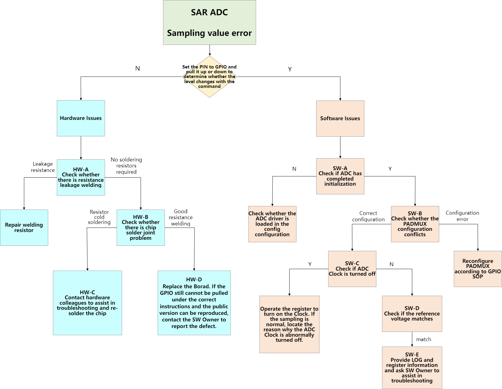
2. Explanation of the Debug Flow for Incorrect ADC Sampling Values
2.1 Hardware Issues
When incorrect ADC sampling values are detected, you can manipulate registers or use GPIO commands to set the corresponding PIN to GPIO and toggle it high and low (note that some PINs may not have GPIO functionality as the highest priority, in which case you need to clear higher priority settings first). If the actual output level does not change, it can be determined to be a hardware issue, and you can troubleshoot in the following order:
2.1.1 HW-A Check Resistors
Check if there are any soldering issues with the corresponding PIN in the schematic; if there is a cold solder joint, it needs to be re-soldered, otherwise the PIN will not be functional.
2.1.2 HW-B Check Soldering Conditions
If the GPIO can toggle high and low after changing the Board, it may indicate a cold solder joint on the chip, requiring rework.
2.1.3 HW-C Request Assistance
Contact hardware colleagues for assistance in troubleshooting and re-soldering the chip.
2.1.4 HW-D Issue Reporting
If the GPIO still cannot toggle high and low after changing the Board, please contact FAE to report the issue.
2.2 Software Issues
2.2.1 Step SW-A Check ADC Initialization and Usage
On the Linux side, check if the interfaces for SAR ADCLP and ADCMP exist under sysfs (refer to section 7.4.1 of the ADCLP usage reference and ADCMP usage reference); if they do not exist, it indicates that the IP has not been initialized properly.
If initialization is not completed, data cannot be obtained. Please check if the config and DTS configurations have loaded the corresponding ADC drivers.
Linux config:
Device Drivers --->
    SStar SoC platform drivers --->
        <*> Sstar ADCMP driver
        <*> Sstar ADCLP driver
Linux DTS:
adclp0: adclp0@1f002800 {
    compatible = "sstar,adclp";
    reg = <0x0 0x1F002800 0x0 0x200>;
    ......
    status = "ok";    //ok: initialized adclp
};
.....
adcmp0: adcmp@1f00ac00 {
    compatible = "sstar,adcmp";
    reg = <0x0 0x1F00AC00 0x0 0x200>, <0x0 0x1F00AE00 0x0 0x200>, <0x0 0x1F003C00 0x0 0x200>,
            <0x0 0x1F204600 0x0 0x200>, <0x0 0x1F203E00 0x0 0x200>;
    ......
    status = "ok";    //ok: initialized adcmp
};
On the Riscv side, please check if the ADC configuration in pcupid-default.sys is correct (refer to section 6.3 of the RISCV_ADCLP usage reference and RISCV_ADCMP usage reference), noting that when enabling DMA functionality for ADCMP, both dma_en_u8 and interrupts_en_u8 need to be set to 1.
<adclp4>
    [reg_u32] 0x2002800;
    [interrupts_u32] INT_PM_IRQ_SAR_KP;
    [camclk_u16] CAMCLK_sar;
    [interrupts_en_u8] 1;
    [ref_vol_u32] 1800;
    [upper_bound_u16] 0x3FF;
    [lower_bound_u16] 0;
    [status_u8] 1; /*1, enable ADCLP channel4*/

<adcmp0>
    [reg_u32] 0x200AC00, 0x200AE00, 0x2003C00, 0x2204600, 0x2203E00;
    [interrupts_u32] INT_PM_FIQ_ADCMP;
    [camclk_u16] CAMCLK_pm_pwm_adc;
    [interrupts_en_u8] 0;
    [dma_en_u8] 0;
    [dma_count_u32] 50;
    [clk_level_u8] 0;
    [ref_vol_u32] 1800;
    [regular_method_u8] 0;
    [inject_method_u8] 0;
    [regular_ch_u8] 0, 1, 2, 3, 4, 5, 6, 7, 8, 9, 10, 11;
    [inject_ch_u8] 12, 13, 14, 15, 16, 17, 18, 19, 20, 21;
    [upper_bound_u16] 0xFFFF, 0xFFFF, 0xFFFF, 0xFFFF, 0xFFFF, 0xFFFF, 0xFFFF, 0xFFFF, 0xFFFF, 0xFFFF, 0xFFFF,
                    0xFFFF, 0xFFFF, 0xFFFF, 0xFFFF, 0xFFFF, 0xFFFF, 0xFFFF, 0xFFFF, 0xFFFF, 0xFFFF, 0xFFFF;
    [lower_bound_u16] 0, 0, 0, 0, 0, 0, 0, 0, 0, 0, 0, 0, 0, 0, 0, 0, 0, 0, 0, 0, 0, 0;
    [status_u8] 1; /*1, enable ADCMP group0*/

<adcmp1>
    [reg_u32] 0x2203600, 0x2203A00, 0x2200E00, 0x2204600, 0x2203E00;
    [interrupts_u32] INT_FIQ_ADCMP;
    [camclk_u16] CAMCLK_pwm_adc;
    [interrupts_en_u8] 0;
    [dma_en_u8] 0;
    [dma_count_u32] 50;
    [clk_level_u8] 3;
    [ref_vol_u32] 1800;
    [regular_method_u8] 0;
    [inject_method_u8] 0;
    [regular_ch_u8] 0, 1;
    [upper_bound_u16] 0xFFFF, 0xFFFF;
    [lower_bound_u16] 0, 0;
    [status_u8] 1; /*1, enable ADCMP group1*/
Check if the same group of ADCMP or the same channel of ADCLP is configured on both the LINUX and RISCV sides. If configured on both sides, the configuration needs to be removed from the unused side.
Check if the ADC usage method is correct; a common issue is related to the triggering method.
When the ADCMP is set to trigger by PWM (0~11) without pre-setting the corresponding PWM's dead time, it will not trigger, resulting in no data.
For specific usage methods of ADC on the LINUX side, refer to the usage documentation ADCLP usage reference and ADCMP usage reference, and for the RISCV side, refer to the usage documentation RISCV_ADCLP usage reference and RISCV_ADCMP usage reference.
2.2.2 Step SW-B Check PADMUX
Check if there are any conflicts in PADMUX; refer to the PADMUX conflict check content in Gpio_DebugSop. If both ARM and RISCV are used simultaneously, both sides need to be checked together.
2.2.3 Step SW-C Check CLK Configuration
Check if the ADC CLK is properly enabled. The registers for checking each ADC clock are as follows; read the instruction/customer/riu_r 0x1038 0x38, where a corresponding bit of 0 indicates the clock is properly enabled, and a bit of 1 indicates the clock is off.
| ADC | BANK | OFFSET | BIT |
|---|---|---|---|
| ADCMP channel0-17 | 1038 | 38 | bit0 |
| ADCMP channel18-19 | E | 24 | bit0 |
| ADCLP | E | 22 | bit5 |
If the clock is off, check the clock configuration in pcupid-clks.dtsi. Setting auto_enable = <1> indicates that the clock will remain on after the system starts; when both RISCV and LINUX need to use the same group of ADCMP, this configuration is required. Setting ignore = <1> indicates that the clock is controlled by the module itself; when only RISCV is using the ADC, the LINUX side configuration should be removed according to this configuration.
2.2.4 Step SW-D Check Reference Voltage
Check if the external voltage input to the ADC matches the set reference voltage; if they do not match, ensure that the external voltage is within the reference voltage range.
2.2.5 Step SW-E Request Assistance
If all the above steps are checked and OK, please <font color=blue>provide ADC-related LOG and ADC configuration information </font>, and contact FAE for debugging assistance.
3. Common Issues Explanation
3.1 Slow Voltage Change of ADCMP Sampling Components Leading to Incorrect Sampling Values
This is common with infrared ranging components, where the voltage drop time may exceed the sampling time of ADCMP. You can adjust the sampling time point by trying the following two solutions:
-
Set the PWM to polarity 1, add the channels of the devices with slow falling edges to inject mode, while adding the others without special requirements to regular mode to ensure accurate sampling (note that inject uses single trigger; using continue will cause regular channels to be unable to sample).
-
Set the PWM to polarity 0, add the channels of the devices with slow falling edges to inject mode, and set the inject delay count (delay duration = pwm source clock * count) to postpone the sampling timing.
3.2 ADCMP Sampling Results Varying by Multiples of 256
When the input voltage of a certain ADC channel corresponding to the PIN exceeds the reference voltage, the sampling of the previous channel will be interfered with, and the sampling result can only be a multiple of 256.
adcmp0: adcmp@1f00ac00 {
    compatible = "sstar,adcmp";
    reg = <0x0 0x1F00AC00 0x0 0x200>, <0x0 0x1F00AE00 0x0 0x200>, <0x0 0x1F003C00 0x0 0x200>, <0x0 0x1F204600 0x0 0x200>, <0x0 0x1F203E00 0x0 0x200>;
    clocks = <&CLK_pm_pwm_adc>;
    interrupt-parent = <&sstar_pm_main_intc>;
    interrupts = <INT_PMSLEEP_FIQ_ADC>;
    interrupts-enable;
    group = <0>;
    //dma-enable;
    //dma-count = <50>;
    ref-voltage = <1800>;//1.5V 1.8V
    //0:24M 1:12M
    clk-select = <0>;
    regular-method = <0>;
    inject-method = <0>;
    regular-ch = <0 1 2 8 3 9 4 5 6 7 10 11 12 13 14 15 16 17 18 19 20 21>;
    upper-bound = <0xFFFF 0xFFFF 0xFFFF 0xFFFF 0xFFFF 0xFFFF 0xFFFF 0xFFFF 0xFFFF 0xFFFF 0xFFFF 0xFFFF 0xFFFF 0xFFFF 0xFFFF 0xFFFF 0xFFFF 0xFFFF 0xFFFF 0xFFFF 0xFFFF 0xFFFF>;
    lower-bound = <0 0 0 0 0 0 0 0 0 0 0 0 0 0 0 0 0 0 0 0 0 0>;
    status = "okay";
};
For example, in the above configuration, if the ref-voltage is 1.8V, and the input voltages of channels 8 and 9 exceed 1.8V, then the sampling results of channels 2 and 3 will be interfered with and can only be multiples of 256.
3.3 Inaccurate ADCMP Sampling
-
Check if the pins are in GPIO mode; refer to the "Get GPIO Enable Status" section in
Gpio_DebugSop. -
Operate GPIO before each sampling to use it as a trigger source, capturing the ADC sampling timing and determining the input voltage state at that sampling point; the ADC sampling interval is short, so wait for the voltage to stabilize before sampling; additionally, the input voltage should be sourced from an LDO processed input; if it is from a DCDC power supply, there may be significant ripple.
-
When the input current is low, there may be significant deviations in multiple samples; ensure that the input current is sufficient.
-
The Riscv debug port uses PAD_UART0_RX/TX, which is in the same power domain as the 5M ADC's 2 channels, and the layout may cause interference with the ADC; in the PCUPID platform Riscv environment, issuing commands via the serial port may show spikes in ADCMP input, with a frequency matching the command actions; at this time, switch to the ARM debug port to avoid interference.