RISVC_SPWM USER GUIDE
REVISION HISTORY
| Revision No. | Description |
Date |
|---|---|---|
| 1.0 | 09/06/2024 | |
| 1.1 | 04/14/2025 |
1. OVERVIEW
SPWM (Sinusoidal Pulse Width Modulation) is a pulse width modulation technology commonly used in AC motor drive and inverter control. It achieves precise control of AC motor speed and power by converting DC voltage into AC voltage close to a sine waveform.
SPWM technology is based on the PWM (Pulse Width Modulation) principle, but unlike traditional square wave PWM, it uses a series of narrow pulses to simulate a sine waveform. The pulse width and frequency of these narrow pulses can be reasonably adjusted to produce an output close to a sine wave.
1.1. Modulation Process
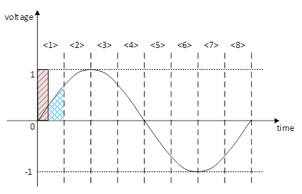
Taking the carrier frequency as 8 times the sine wave frequency (i.e., modulation index = 8) as an example, the modulation process can be explained as follows:
The sine wave is divided into eight equal segments and each segment is marked with a number <1> to <8>;
According to the principle of equal area in automatic control, the duty cycle of the square wave (the red highlighted part) is adjusted so that its area matches the area under the sine wave (the blue highlighted part) in each interval. For example, as shown in the interval <1> in the figure, the control effect on the motor is equivalent.
In this way, we can achieve the same control effect as a sine wave by using a series of square waves.
1.2. Motor Control
Take a two-phase and four-wire motor as an example, there are four terminals: A-, A+, B- and B+. A- and A+ combine to form a sine wave for phase A, while B- and B+ combine to form a sine wave for phase B. The phase difference between phase A and phase B is 90°. The higher the frequency of the sine wave, the faster the motor speed.
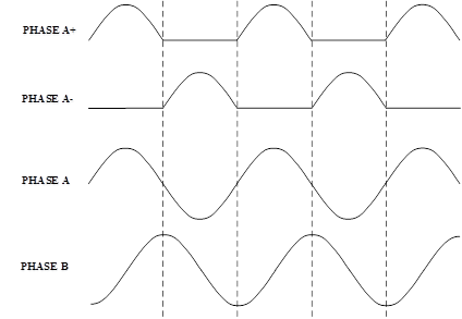
Three-phase motors are similar to two-phase motors, the main difference is that three-phase motors have three phases, and the phase difference between adjacent phases is 60°.
2. FUNCTION DESCRIPTION
-
The number of channels supporting SPWM is 18, of which channels 0~17 need to be added to their own groups. For details, see Correspondence between Group and Channel. Under normal circumstances, 4 channels or 6 channels need to be added to the group. From the perspective of motor control, it supports up to 3 two-phase four-wire motors and 1 three-phase six-wire motor (if 4 two-phase four-wire motors are used, the remaining two channels can be used as PWM).
-
The SPWM carrier frequency is 50Hz~50KHz, and the supported OSCCLK (Hz) is: 86M, 24M, 12M, 6M, 3M, 1.5M, 750K.
-
The sine wave cannot be distorted, that is, the new configuration of the period and duty cycle will take effect only after the current sine wave period ends.
-
The modulation modes supported by SPWM are
Full-wave mode,Half-wave modeandSymmetric half-wave mode, the corresponding maximum modulation index is 64, 128 and 256. -
The same group of SPWMs share a duty table, supporting up to 16bits * 64 duty configurations, that is, one modulation cycle supports up to 64 different duty cycle settings.
-
Support phase adjustment, that is, you can select any duty in the duty table as the starting point to start outputting SPWM.
-
Support scale function, that is, you can configure the scaling ratio for all duties in the duty table, which can be used to adjust the amplitude of the modulation wave.
-
Support clamp function, that is, you can set a clamp on the duty cycle. When duty <= lower limit, the duty cycle is 0, and when duty >= upper limit, the duty cycle is 100%, which can be used for dead zone protection.
-
Support round function, that is, SPWM in the same group will stop after generating a specific number of pulses.
-
Support stop function, that is, SPWM in the same group will stop urgently.
3. RELATED CONCEPT DESCRIPTION
3.1. Modulation Mode and Modulation Index
-
Full-wave mode
The maximum value of a sine cycle is 64 carrier cycles (the modulation index can be set to 64 at most), and each carrier cycle is effective for duty, and the duty cycle is output according to the setting order of the duty table.
-
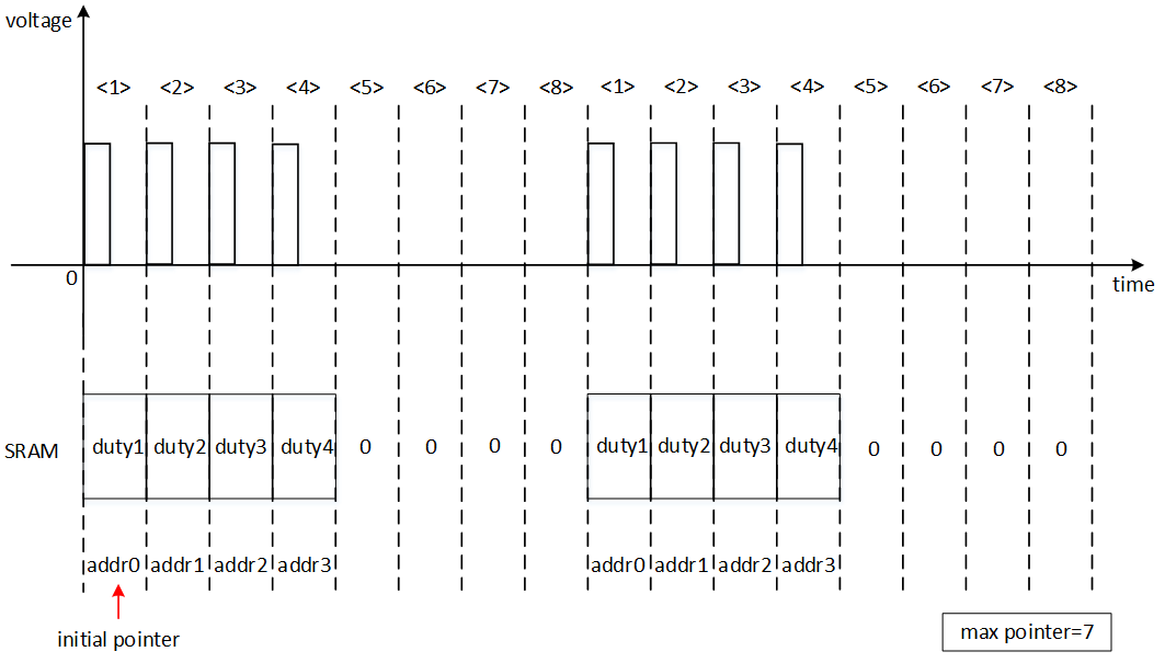
Half-wave mode
The maximum value of a sine cycle is 128 carrier cycles (the modulation index can be set to 128 at most), the first 64 carrier cycles are effective for duty, and the duty cycle is output according to the setting order of the duty table, and the duty of the last 64 carrier cycles is 0.
-
Symmetric half-wave mode
The maximum value of a sine cycle is 256 carrier cycles (the modulation index can be set to 256 at most). The 1st to 64th carrier cycles are all effective for duty, and the duty cycle is output according to the setting order of the duty table. The 65th to 128th carrier cycles are all effective for duty, and the duty cycle is output in the opposite order of the duty table setting, which is symmetrical with the first 64 carrier cycles. The duty of the 128th to 256th carrier cycle is 0.
-
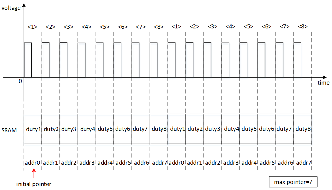
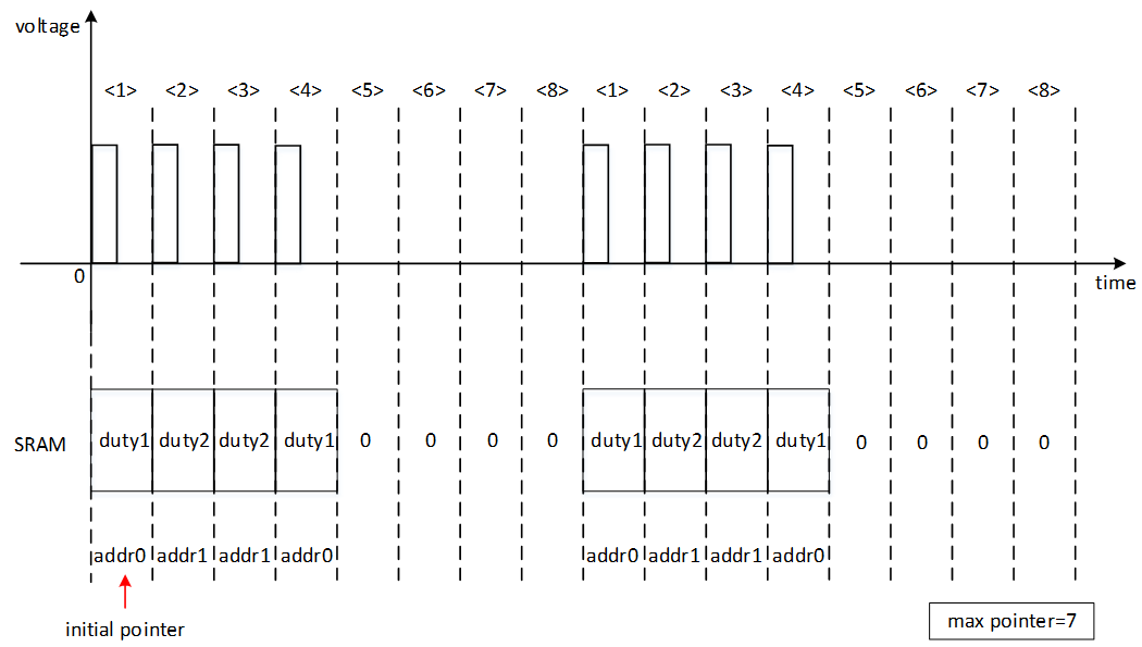
Duty Table
Each group of spwm shares a duty table, which can be abstractly understood as an array, which can store up to 64 duty values. When spwm is enabled, it will output the corresponding duty in each carrier cycle sequentially in the order of the duty table;
Taking
Full-wave modeas an example, if the modulation index is set to 10 and the initial phase is 0, then spwm will output waveforms according to duty0~duty9 in the duty table; if the modulation index is set to 64, then spwm will output waveforms according to duty0~duty63 in the duty table; the modulation index ofFull-wave modedoes not support setting values greater than 64;Taking
Half-wave modeas an example, if the modulation index is set to 10 and the initial phase is 0, then spwm will output waveforms according to duty0~duty9 in the duty table for the 1st to 10th carrier cycles, and the duty of the 11th to 20th carrier cycles is 0; if the modulation index is set to 128, then spwm will output waveforms according to duty0~duty63 in the duty table for the 1st to 64th carrier cycles, and the duty of the 65th to 128th carrier cycles is 0; the modulation index ofHalf-wave modedoes not support setting values greater than 128.
3.2. Scale Function
The duty cycle scaling function can quickly adjust the amplitude of the modulation wave.
Assuming OSCCLK is 12MHz, carrier period is 50KHz, and the scaling ratio set by scale is 50% of the original, the change of duty is as follows:
| Duty index | Original duty cycle | Duty cycle reduced by 50% |
|---|---|---|
| 0 | 250 ns | 83 ns |
| 1 | 500 ns | 250 ns |
| 2 | 750 ns | 335 ns |
| 3 | 1000 ns | 500 ns |
| 4 | 1250 ns | 585 ns |
| 5 | 1500 ns | 750 ns |
| 6 | 1750 ns | 835 ns |
| 7 | 2000 ns | 1000 ns |
| 8 | 2250 ns | 1085 ns |
| 9 | 2500 ns | 1250 ns |
Please note that the duty cycle is an integer multiple of 12MHz, so after the scale conversion, the duty cycle that is not an integer multiple will be rounded down.
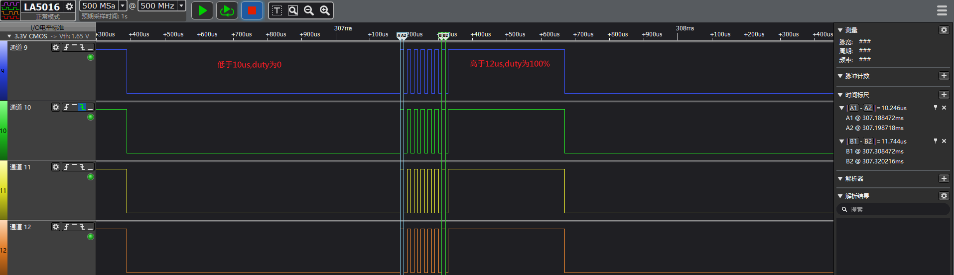
3.3. Clamp Function
Duty cycle clamp mode, when duty <= lower limit, the duty cycle is 0, when duty >= upper limit, the duty cycle is 100%.
With OSCCLK of 12MHz, carrier period of 50KHz, duty cycle range set by duty table of 250ns~16000ns, and duty cycle clamp upper and lower limits set to 10000~12000ns, the output waveform is as follows:
3.4. GROUP Related Concepts
3.4.1 Sync mode
Sync mode can add each spwm channel to its own group to complete the purpose of controlling multiple spwm at the same time. A group has 4 or 6 spwm channels, and the group and channel correspondence is as follows:
| Group | Group Member |
|---|---|
| Group0 | SPWM0, SPWM1, SPWM2, SPWM3 |
| Group1 | SPWM4, SPWM5, SPWM6, SPWM7 |
| Group2 | SPWM8, SPWM9, SPWM10, SPWM11 |
| Group3 | SPWM12, SPWM13, SPWM14, SPWM15, SPWM16, SPWM17 |
You can choose whether to add spwm to the Group through SYSDESC configuration:
<pwm0>
    [reg_u32_u16] 0x2203200 0x40;
    ......
    [group_u32] 0xFFFF;
    [spwm_group_u32] 0;
    ......

<pwm1>
    [reg_u32_u16] 0x2203240 0x40;
    ......
    [group_u32] 0xFFFF;
    [spwm_group_u32] 0;
    ......

<pwm2>
    [reg_u32_u16] 0x2203280 0x40;
    ......
    [group_u32] 0xFFFF;
    [spwm_group_u32] 0;
    ......

<pwm3>
    [reg_u32_u16] 0x22032C0 0x40;
    ......
    [group_u32] 0xFFFF;
    [spwm_group_u32] 0;
    ......

<pwm4>
    [reg_u32_u16] 0x2203400 0x40;
    ......
    [group_u32] 1;
    [spwm_group_u32] 0xFFFF;
    ......

<pwm5>
    [reg_u32_u16] 0x2203440 0x40;
    ......
    [group_u32] 1;
    [spwm_group_u32] 0xFFFF;
    ......

<pwm6>
    [reg_u32_u16] 0x2203480 0x40;
    ......
    [group_u32] 1;
    [spwm_group_u32] 0xFFFF;
    ......

<pwm7>
    [reg_u32_u16] 0x22034C0 0x40;
    ......
    [group_u32] 1;
    [spwm_group_u32] 0xFFFF;
    ......

<pwm8>
    [reg_u32_u16] 0x2203800 0x40;
    ......
    [group_u32] 0xFFFF;
    [spwm_group_u32] 0xFFFF;
    ......

<pwm9>
    [reg_u32_u16] 0x2203840 0x40;
    ......
    [group_u32] 0xFFFF;
    [spwm_group_u32] 0xFFFF;
    ......
SYSDESC PWM nodes are configured with spwm_group_u32 to enable the spwm function and join the spwm group. For example, if pwm0~pwm3 are all configured with [spwm_group_u32] 0 and [group_u32] 0xFFFF, then pwm0~pwm3 will be given the spwm function and join spwm group0. It is necessary to follow the characteristics and settings of spwm, so spwm_group_u32 can be understood as the function switch of spwm;
SYSDESC PWM nodes are configured with group_u32 to enable the pwm function and join the pwm group. For example, if pwm4~pwm7 are all configured with [group_u32] 1 and [spwm_group_u32] 0xFFFF, then pwm4~pwm7 will be given the pwm function and join pwm group1. At this time, the spwm function cannot be used;
SYSDESC PWM nodes are configured with [group_u32] 0xFFFF and [spwm_group_u32] 0xFFFF, such as pwm8 and pwm9, then pwm8 and pwm9 can only be used as the ordinary pwm.
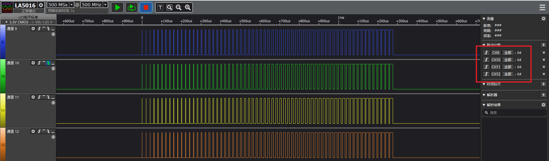
3.4.2 Round mode
The round function will stop after all spwm channels in the same spwm group complete a certain number of pulses. Each spwm group has its own independent round function. As shown in the figure below, spwm group0 uses full wave mode and round is set to 64, so the waveform stops after 64 pulses are actually output.
3.4.3 Stop mode
The stop function can stop all spwm channels in the current spwm group immediately (without waiting for the current cycle to complete) and maintain the level at the end. Each spwm group has its own independent stop function.
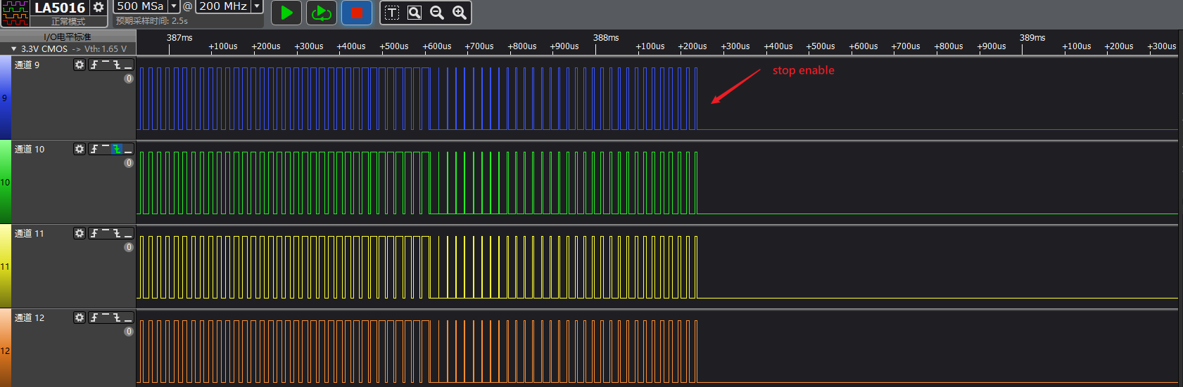
Note: It is not recommended to set the stop time to be too long, especially when the level is maintained at a high level after stopping.
4. Hardware connection instructions
After the PIN pin is multiplexed to PWM MODE, it is already in output state. To protect the circuit, please do not inject external voltage; at the same time, the hardware will output PWM waveform or SPWM waveform according to the register setting, and the load can be connected as needed
5. RISCV USAGE INTRODUCTION
5.1. DRIVER PATH
sc/driver/sysdriver/pwm/drv/pub/drv_pwm.h
sc/driver/sysdriver/pwm/drv/src/drv_pwm.c
sc/driver/sysdriver/pwm/drv/src/drv_spwm_test.c
sc/driver/sysdriver/pwm/hal/chipname/src/hal_pwm.c
sc/driver/sysdriver/pwm/hal/chipname/inc/hal_pwm.h
sc/driver/sysdriver/pwm/hal/chipname/inc/hal_pwm_cfg.h
5.2. CONFIG Configuration
The config file is located in mak/options_chipname_riscv_isw.mak. Enable CONFIG_PWM_SUPPORT, CONFIG_SSTAR_SPWM and CONFIG_SSTAR_PWM_EXTEND.
# Feature_Name = [DRV] PWM driver support
# Description = PWM driver support
# Option_Selection = TRUE, FALSE
CONFIG_PWM_SUPPORT = TRUE       //Enable the PWM driver
CONFIG_SSTAR_SPWM  = TRUE       //Enable the SPWM function
CONFIG_SSTAR_PWM_EXTEND = TRUE  //SPWM only supports the high-precision mode
5.3. SYSDESC Configuration
The file chipname_xxx.sys is used to describe the hardware attributes of peripherals. The attribute values contained in the peripheral node can be used to configure the peripherals, similar to the Linux device tree. The file is located in sc/driver/sysdriver/sysdesc/hal/chipname/pub. The following takes pwm0 as an example:
<pwm0>
    [reg_u32_u16] 0x2203200 0x40;
    [interrupts_u32] INT_IRQ_PWM_GROUP0;
    [camclk_u16] CAMCLK_pwm;
    [group_u32] 0xFFFF;
    [spwm_group_u32] 0;
    [clk_level_u8] 0;
    [status_u8] 0;
The attributes supported for configuration in the pwm driver are as follows:
| Attribute | Description | Setting value | Remark |
|---|---|---|---|
| reg_u32_u16 | Specify the bank address | 0x2203200 | Modification prohibited |
| interrupts_u32 | Specify the hardware interrupt number | INT_IRQ_PWM_GROUP0 | Modification prohibited |
| camclk_u16 | Specify the clock source | CAMCLK_pwm | Modification prohibited |
| group_u32 | Select whether to join the pwm group | To enable spwm, this attribute must be set to 0xFFFF | You can only choose to join group or spwm group |
| spwm_group_u32 | Select whether to join the pwm group | According to Group and channel correspondence, the corresponding group index is assigned. 0xFFFF means not to join | You can only choose to join group or spwm group |
| clk_level_u8 | Select the clock source | Pwm0~17 can be selected from 0~6 corresponding to 12M/6M/3M/1.5M/750K/86M/24M | Pwm0~17 selections must be consistent |
| status_u8 | Select whether to enable the driver | 1: enable; 0: disable | Can be modified as needed |
5.4. PADMUX Configuration
CONFIG Configuration: CONFIG_PADMUX_SUPPORT=TRUE
If the chipname_xxx.sys file is configured with the attribute <padmux>, then the PADMUX setting is directly configured here:
<padmux>
    [schematic_u32_u32_u32]
              PAD_GPIOC_00   PINMUX_FOR_PWM0_MODE_1    MDRV_PUSE_PWM0,
              PAD_GPIOC_01   PINMUX_FOR_PWM1_MODE_1    MDRV_PUSE_PWM1,
              PAD_GPIOC_02   PINMUX_FOR_PWM2_MODE_1    MDRV_PUSE_PWM2,
              PAD_GPIOC_03   PINMUX_FOR_PWM3_MODE_1    MDRV_PUSE_PWM3,
              PAD_GPIOC_04   PINMUX_FOR_PWM4_MODE_1    MDRV_PUSE_PWM4,
              PAD_GPIOC_05   PINMUX_FOR_PWM5_MODE_1    MDRV_PUSE_PWM5,
              PAD_GPIOC_06   PINMUX_FOR_PWM6_MODE_1    MDRV_PUSE_PWM6,
              PAD_GPIOC_07   PINMUX_FOR_PWM7_MODE_1    MDRV_PUSE_PWM7,
              PAD_GPIOC_08   PINMUX_FOR_PWM8_MODE_1    MDRV_PUSE_PWM8,
              PAD_OUTP_CH0   PINMUX_FOR_PWM9_MODE_1    MDRV_PUSE_PWM9,
              PAD_GPIOA_00   PINMUX_FOR_PWM10_MODE_2   MDRV_PUSE_PWM10,
              PAD_GPIOA_01   PINMUX_FOR_PWM11_MODE_2   MDRV_PUSE_PWM11,
              PAD_GPIOA_02   PINMUX_FOR_PWM12_MODE_2   MDRV_PUSE_PWM12,
              PAD_GPIOA_03   PINMUX_FOR_PWM13_MODE_2   MDRV_PUSE_PWM13,
              PAD_GPIOA_04   PINMUX_FOR_PWM14_MODE_2   MDRV_PUSE_PWM14,
              PAD_GPIOA_05   PINMUX_FOR_PWM15_MODE_2   MDRV_PUSE_PWM15,
              PAD_GPIOA_06   PINMUX_FOR_PWM16_MODE_2   MDRV_PUSE_PWM16,
              PAD_GPIOA_07   PINMUX_FOR_PWM17_MODE_2   MDRV_PUSE_PWM17,
              ......
    [status_u8] 1;
Otherwise, enable the PADMUX driver and configure the pin multiplexing function in the chipname-xxx-padmux.c file, which is located in sc/driver/sysdriver/padmux/hal/chipname/src. You only need to add the following content to the corresponding schematic attribute:
pad_info_t schematic[] =
{
      {PAD_GPIOC_00   PINMUX_FOR_PWM0_MODE_1    MDRV_PUSE_PWM0},
      {PAD_GPIOC_01   PINMUX_FOR_PWM1_MODE_1    MDRV_PUSE_PWM1},
      {PAD_GPIOC_02   PINMUX_FOR_PWM2_MODE_1    MDRV_PUSE_PWM2},
      {PAD_GPIOC_03   PINMUX_FOR_PWM3_MODE_1    MDRV_PUSE_PWM3},
      {PAD_GPIOC_04   PINMUX_FOR_PWM4_MODE_1    MDRV_PUSE_PWM4},
      {PAD_GPIOC_05   PINMUX_FOR_PWM5_MODE_1    MDRV_PUSE_PWM5},
      {PAD_GPIOC_06   PINMUX_FOR_PWM6_MODE_1    MDRV_PUSE_PWM6},
      {PAD_GPIOC_07   PINMUX_FOR_PWM7_MODE_1    MDRV_PUSE_PWM7},
      {PAD_GPIOC_08   PINMUX_FOR_PWM8_MODE_1    MDRV_PUSE_PWM8},
      {PAD_OUTP_CH0   PINMUX_FOR_PWM9_MODE_1    MDRV_PUSE_PWM9},
      {PAD_GPIOA_00   PINMUX_FOR_PWM10_MODE_2   MDRV_PUSE_PWM10},
      {PAD_GPIOA_01   PINMUX_FOR_PWM11_MODE_2   MDRV_PUSE_PWM11},
      {PAD_GPIOA_02   PINMUX_FOR_PWM12_MODE_2   MDRV_PUSE_PWM12},
      {PAD_GPIOA_03   PINMUX_FOR_PWM13_MODE_2   MDRV_PUSE_PWM13},
      {PAD_GPIOA_04   PINMUX_FOR_PWM14_MODE_2   MDRV_PUSE_PWM14},
      {PAD_GPIOA_05   PINMUX_FOR_PWM15_MODE_2   MDRV_PUSE_PWM15},
      {PAD_GPIOA_06   PINMUX_FOR_PWM16_MODE_2   MDRV_PUSE_PWM16},
      {PAD_GPIOA_07   PINMUX_FOR_PWM17_MODE_2   MDRV_PUSE_PWM17},
      ......
};
The first column is the pin index number, which can be queried in sc/drivers/sysdriver/gpio/hal/chipname/pub/gpio.h;
The second column is the mode definition, which can be queried in sc/drivers/sysdriver/gpio/hal/chipname/pub/padmux.h;
The third column is the index name of the pin and matching mode, which can be queried in sc/drivers/sysdriver/padmux/drv/pub/drv_puse.h.
5.5. Sample Code
The demo source code is located in sc/driver/sysdriver/pwm/drv/src/drv_spwm_test.c.
6. API Reference
The header file is located in sc/driver/sysdriver/pwm/drv/pub/drv_pwm.h.
struct spwm_gp_cfg
{
    u8  mode;       //Modulation mode
    u8  step;       //Initial phase
    u8  scale;      //Duty scaling ratio n, calculated as n/8
    u32 group;      //SPWM group id
    u8  enable;     //1: enable
    u64 period;     //SPWM carrier period, in ns
    u8  clamp_en;   //Enable duty clamp function
    u8  duty_len;   //Duty table length
    u64 duty[64];   //Duty table setting, up to 64
    u32 round_num;  //Set the number of round pulses
    u64 clamp_max;  //Clamp upper limit
    u64 clamp_min;  //Clamp lower limit
};

extern int drv_spwm_update_period(u32 group, u64 period);
extern int drv_spwm_set_sram_duty(u32 group, u8 index, u64 duty_ns);
extern int drv_spwm_update_duty(u32 group, u8 index, u8 len, u64 *duty_ns);
extern int drv_spwm_set_group_config(struct spwm_gp_cfg *gp_cfg);
extern int drv_spwm_get_group_config(struct spwm_gp_cfg *gp_cfg);
extern int drv_spwm_stop_enable(u32 group, u8 stop_en);
extern int drv_spwm_round_enable(u32 group, u32 round_num);
6.1 drv_spwm_set_group_config
-
Purpose
Configure spwm group attributes.
-
Syntax
int drv_spwm_set_group_config(struct spwm_gp_cfg *gp_cfg)
-
Parameter
Parameter name Description gp_cfg Used to configure the spwm group's modulation mode, initial phase, duty table, carrier period and other attributes -
Return value
Result Description Success Return 0 Failure Return negative numbers
6.2 drv_spwm_get_group_config
-
Purpose
Get the attribute configuration of the current spwm group.
-
Syntax
int drv_spwm_get_group_config(struct spwm_gp_cfg *gp_cfg)
-
Parameter
Parameter name Description gp_cfg Used to get the spwm group's modulation mode, initial phase, duty table, carrier period and other attributes -
Return value
Result Description Success Return 0 Failure Return negative numbers
6.3 drv_spwm_update_period
-
Purpose
Update the carrier period of the spwm group.
-
Syntax
int drv_spwm_update_period(u32 group, u64 period)
-
Parameter
Parameter name Description group Select the group to enable the spwm waveform period Carrier period, in ns -
Return value
Result Description Success Return 0 Failure Return negative numbers
6.4 drv_spwm_set_sram_duty
-
Purpose
Update the single duty value of the specified subscript in the spwm duty table.
-
Syntax
int drv_spwm_set_sram_duty(u32 group, u8 index, u64 duty_ns)
-
Parameter
Parameter name Description group Select the group to enable the spwm waveform index Select the subscript of the duty table duty_ns Set the duty cycle in ns -
Return value
Result Description Success Return 0 Failure Return negative numbers
6.5 drv_spwm_update_duty
-
Purpose
Update the length duty values of the specified subscript in the spwm duty table.
-
Syntax
int drv_spwm_update_duty(u32 group, u8 index, u8 len, u64 *duty_ns);
-
Parameter
Parameter name Description group Select the group to enable the spwm waveform index Select the subscript of the duty table as the starting update point len Set the number of duties to be updated this time duty_ns Address of the duty cycle array -
Return value
Result Description Success Return 0 Failure Return negative numbers
6.6 drv_spwm_stop_enable
-
Purpose
Enable the stop function.
-
Syntax
int drv_spwm_stop_enable(u32 group, u8 stop_en)
-
Parameter
Parameter name Description group Select the group to enable the stop function stop_en 1: enable, waveform stops; 0: disable, waveform resumes -
Return value
Result Description Success Return 0 Failure Return negative numbers
6.7 drv_spwm_round_enable
-
Purpose
Set the number of pwm cycles for round mode operation.
-
Syntax
int drv_spwm_round_enable(u32 group, u32 round_num)
-
Parameter
Parameter name Description group Select the group to enable round mode round_num Specify the number of pwm cycles -
Return value
Result Description Success Return 0 Failure Return negative numbers
7. FAQ
Q1:SPWM Device Does Not Exist
-
Check if the
statusof the SYSDESC PWM node is1. -
Check the
spwm-groupattribute of the SYSDESC PWM node, which should be configured as 0/½/3. -
Check the
groupattribute of the SYSDESC PWM node, which should be configured as 0xFFFF. -
Check if config is configured, see [5.2. CONFIG Configuration].
Q2:No SPWM Waveform is Generated After Configuration
-
First confirm whether the measured pin is correct: open the corresponding schematic to confirm.
-
Confirm whether the corresponding PWM mode is effective. There are two main reasons for pin multiplexing failure:
Reason 1: The pin is not set to PWM mode. See [PADMUX Configuration] for setting methods.
Reason 2: There is a padmux mode with a higher priority than PWM mode is turned on.
-
Check whether the relevant parameters are set successfully.
Call
drv_spwm_get_group_configto get whether the current configuration is correct.