Pwm_DebugSop
REVISION HISTORY
| Revision No. | Description |
Date |
|---|---|---|
| 1.0 | 12/13/2024 |
1. Debug Flowchart
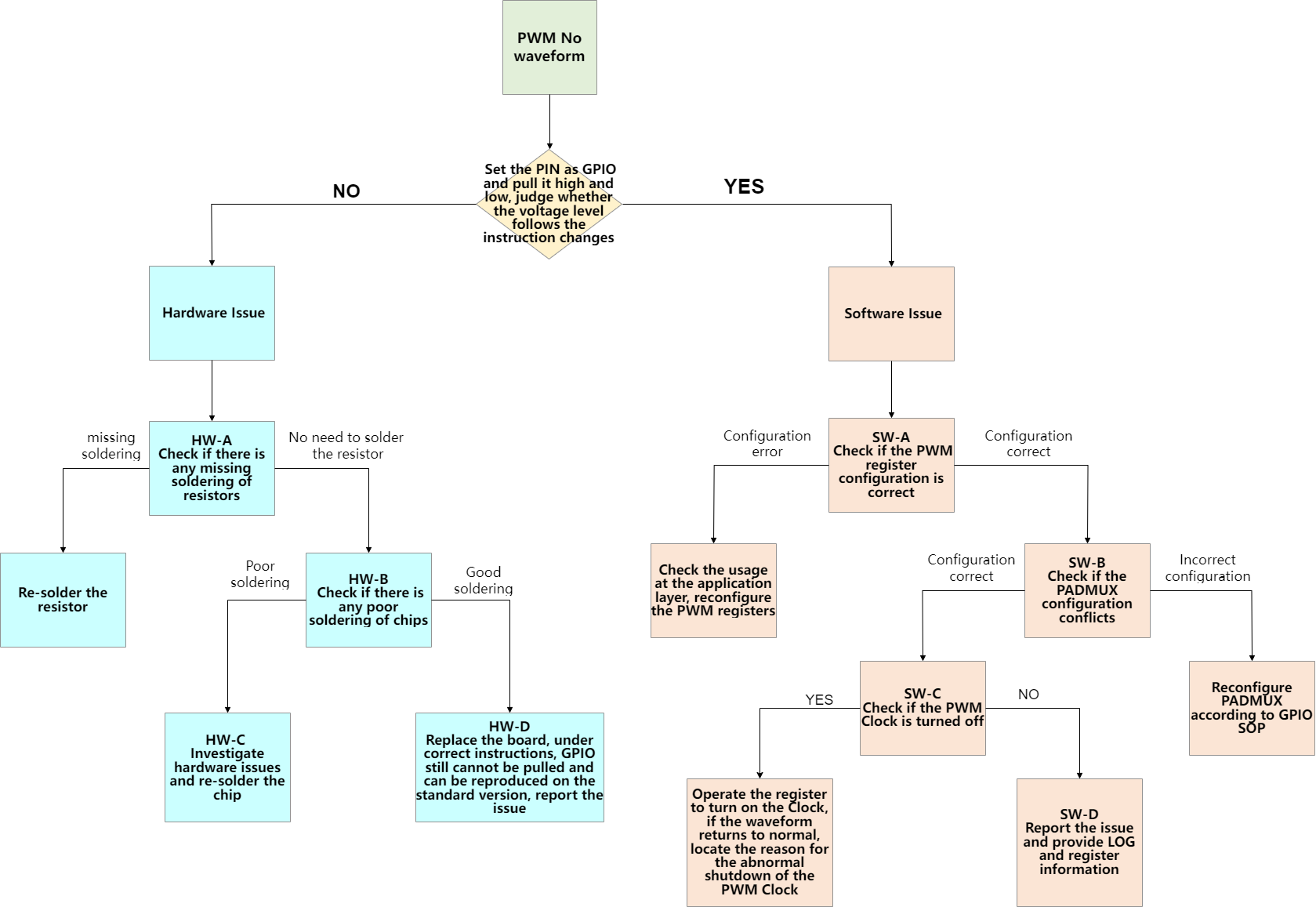
2. Debug Process Description
2.1 Hardware Issues
When PWM is found to have no output waveform, you can operate the registers or GPIO commands to set the corresponding PIN to GPIO and pull it high or low (note that some PINs may not have the highest priority for GPIO functionality, in which case you need to clear the higher priority first). If the actual output level does not change, it can be determined to be a hardware issue, and the following sequence can be used for troubleshooting:
2.1.1 HW-A Check Resistors
Check if there are any soldering issues with the corresponding PIN in the schematic; if there is a cold solder joint, the resistor needs to be re-soldered; otherwise, the PIN will not be connected.
2.1.2 HW-B Check Soldering Conditions
If the GPIO can be pulled high or low after replacing the board, it may be due to a cold solder joint on the chip, requiring rework.
2.1.3 HW-C Request Assistance
Contact hardware colleagues for assistance in troubleshooting and re-soldering the chip.
2.1.4 HW-D Report Issues
If the GPIO still cannot be pulled high or low after replacing the board, contact FAE to report the issue.
2.2 Software Issues
When determined to be a software issue, the following sequence can be used for troubleshooting:
2.2.1 SW-A Check PWM Register Configuration
Dump the PWM bank and check if the register settings are effective, taking PCUPID as an example.
| Channel | Bank | Period Reg | Duty Reg | Shift Reg | Enable Reg | Group status | Group enable |
|---|---|---|---|---|---|---|---|
| PWM0 | 0x1019 | 0x4-0x5 | 0x2-0x3 | 0x0-0x1 | 0x61 BIT0 | 0x64 BIT0 | 0x63 BIT0 |
| PWM1 | 0x1019 | 0x14-0x15 | 0x12-0x13 | 0x10-0x11 | 0x61 BIT1 | 0x64 BIT0 | 0x63 BIT1 |
| PWM2 | 0x1019 | 0x24-0x25 | 0x22-0x23 | 0x20-0x21 | 0x61 BIT2 | 0x64 BIT0 | 0x63 BIT2 |
| PWM3 | 0x1019 | 0x34-0x35 | 0x32-0x33 | 0x30-0x31 | 0x61 BIT3 | 0x64 BIT0 | 0x63 BIT3 |
| PWM4 | 0x101A | 0x4-0x5 | 0x2-0x3 | 0x0-0x1 | 0x61 BIT0 | 0x64 BIT0 | 0x63 BIT0 |
| PWM5 | 0x101A | 0x14-0x15 | 0x12-0x13 | 0x10-0x11 | 0x61 BIT1 | 0x64 BIT0 | 0x63 BIT1 |
| PWM6 | 0x101A | 0x24-0x25 | 0x22-0x23 | 0x20-0x21 | 0x61 BIT2 | 0x64 BIT0 | 0x63 BIT2 |
| PWM7 | 0x101A | 0x34-0x35 | 0x32-0x33 | 0x30-0x31 | 0x61 BIT3 | 0x64 BIT0 | 0x63 BIT3 |
| PWM8 | 0x101C | 0x4-0x5 | 0x2-0x3 | 0x0-0x1 | 0x61 BIT0 | 0x64 BIT0 | 0x63 BIT0 |
| PWM9 | 0x101C | 0x14-0x15 | 0x12-0x13 | 0x10-0x11 | 0x61 BIT1 | 0x64 BIT0 | 0x63 BIT1 |
| PWM10 | 0x101C | 0x24-0x25 | 0x22-0x23 | 0x20-0x21 | 0x61 BIT2 | 0x64 BIT0 | 0x63 BIT2 |
| PWM11 | 0x101C | 0x34-0x35 | 0x32-0x33 | 0x30-0x31 | 0x61 BIT3 | 0x64 BIT0 | 0x63 BIT3 |
| PWM12 | 0x102B | 0x4-0x5 | 0x2-0x3 | 0x0-0x1 | 0x61 BIT0 | 0x64 BIT0 | 0x63 BIT0 |
| PWM13 | 0x102B | 0x14-0x15 | 0x12-0x13 | 0x10-0x11 | 0x61 BIT1 | 0x64 BIT0 | 0x63 BIT1 |
| PWM14 | 0x102B | 0x24-0x25 | 0x22-0x23 | 0x20-0x21 | 0x61 BIT2 | 0x64 BIT0 | 0x63 BIT2 |
| PWM15 | 0x102B | 0x34-0x35 | 0x32-0x33 | 0x30-0x31 | 0x61 BIT3 | 0x64 BIT0 | 0x63 BIT3 |
| PWM16 | 0x102B | 0x44-0x45 | 0x42-0x43 | 0x40-0x41 | 0x61 BIT4 | 0x64 BIT0 | 0x63 BIT4 |
| PWM17 | 0x102B | 0x54-0x55 | 0x52-0x53 | 0x50-0x51 | 0x61 BIT5 | 0x64 BIT0 | 0x63 BIT5 |
| PM PWM0 | 0x1A | 0x4-0x5 | 0x2-0x3 | 0x0-0x1 | 0x7F BIT0 | NA | NA |
| PM PWM1 | 0x1A | 0x14-0x15 | 0x12-0x13 | 0x10-0x11 | 0x7F BIT1 | NA | NA |
If the selected PWM has a Group Status of 0, then the waveform output must satisfy two conditions simultaneously:
Period Reg value > (Duty Reg - Shift Reg) value && Enable Status = 0
If the selected PWM has a Group Status of 1, then the waveform output must satisfy three conditions simultaneously:
Period Reg value > (Duty Reg + Shift Reg) value && Enable Status = 0 && Group Enable = 1
As shown in Figure 2-1, if all configurations are correct, PWM outputs a normal waveform:
period(0x4) = 0x0077, PWM clock = 12Mhz, actual waveform period = 12000000 / (0x0077 + 1) = 100000HZ
duty(0x2) = 0x003B, shift(0x0) = 0x000B, actual waveform duty cycle = (0x003B - 0x000B) / (0x0077 + 1) = 40%
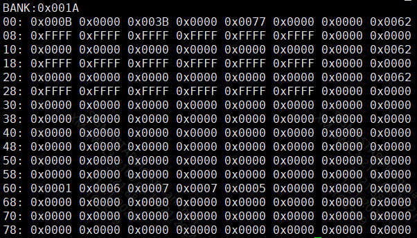
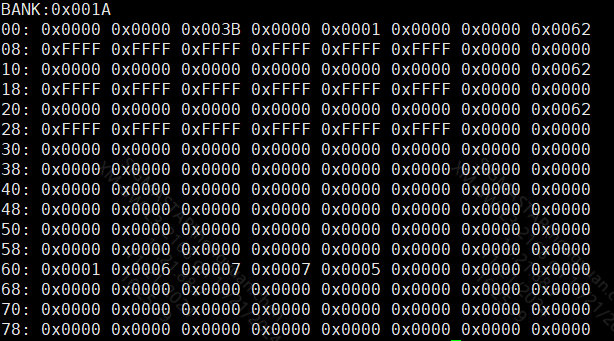
As shown in Figure 2-2, if period < (duty - shift), it cannot output a waveform.
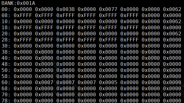
As shown in Figure 2-3, if enable status = 1, it cannot output a waveform.
Since PWM may have different precision modes, using low precision methods to pass parameters in high precision mode may lead to unreasonable PWM register configurations. At this time, confirm the register configuration to backtrack whether the application layer parameters are reasonable.
2.2.2 SW-B Check PADMUX
After checking that the PWM registers are correctly configured and still unable to output a waveform or outputting an abnormal waveform, check if there are any conflicts in PADMUX, see the PADMUX conflict check content in Gpio_DebugSop.
2.2.3 SW-C Check Clock Source
After checking the PWM registers and PADMUX, if it still cannot output a waveform, check whether the PWM Clock has been abnormally turned off, taking PCUPID as an example.
| Channel | Bank | Offset | BIT |
|---|---|---|---|
| PWM0 | 0x1038 | 0x38 | BIT8 |
| PWM1 | 0x1038 | 0x38 | BIT8 |
| PWM2 | 0x1038 | 0x38 | BIT8 |
| PWM3 | 0x1038 | 0x38 | BIT8 |
| PWM4 | 0x1038 | 0x38 | BIT8 |
| PWM5 | 0x1038 | 0x38 | BIT8 |
| PWM6 | 0x1038 | 0x38 | BIT8 |
| PWM7 | 0x1038 | 0x38 | BIT8 |
| PWM8 | 0x1038 | 0x38 | BIT8 |
| PWM9 | 0x1038 | 0x38 | BIT8 |
| PWM10 | 0x1038 | 0x38 | BIT8 |
| PWM11 | 0x1038 | 0x38 | BIT8 |
| PWM12 | 0x1038 | 0x38 | BIT8 |
| PWM13 | 0x1038 | 0x38 | BIT8 |
| PWM14 | 0x1038 | 0x38 | BIT8 |
| PWM15 | 0x1038 | 0x38 | BIT8 |
| PWM16 | 0x1038 | 0x38 | BIT8 |
| PWM17 | 0x1038 | 0x38 | BIT8 |
| PM PWM0 | 0x0E | 0x1C | BIT10 |
| PM PWM1 | 0x0E | 0x1C | BIT10 |
Check whether the BIT of the corresponding channel is 0; 0 indicates that the Clock is enabled, and 1 indicates that it is disabled. At this point, directly operate the register to enable the Clock, and the PWM waveform can be output. This can pinpoint that the issue is entirely related to the Clock. If the clock is off, first check the clock configuration in pcupid-clks.dtsi; setting auto_enable = <1> indicates that the clock remains on after the system starts. When both RISCV and LINUX need to use different channels of PWM, this configuration is necessary; ignore = <1> indicates that the clock is controlled by the module itself. When only RISCV uses PWM, remove the LINUX side configuration according to this configuration.
If there are no issues with the above configuration, provide the PWM Clock information during initialization and the PWM Clock information after enabling PWM to FAE for debugging.
2.2.4 SW-D Request Assistance
If the above steps SW-A, SW-B, and SW-C have all been checked and are OK, please provide the PWM parameter setting records, PWM-related error logs, and PWM BANK information and contact FAE for debugging.
3. Common Issues Description
3.1 PWM Output Frequency Does Not Match Settings
PWM parameters can be in high precision mode (both period and duty cycle in nanoseconds) and low precision mode (period in hertz and duty cycle in percentage). It is possible that parameters are passed in low precision methods while in high precision mode, or that the shift parameter was mistakenly input, leading to a mismatch between the actual output frequency and the expected one. At this time, you can check the registers to backtrack the actual output waveform, as shown below:
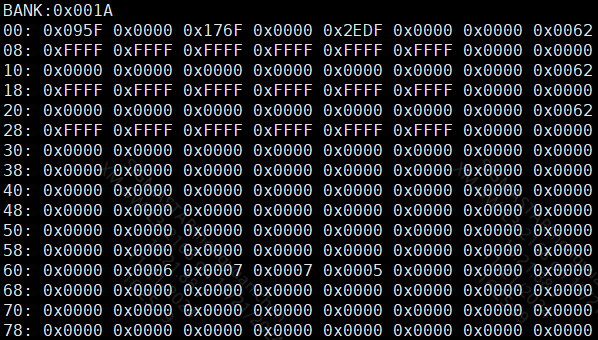
Actual waveform frequency = PWM Clock frequency / (Period Reg + 1) = 12000000 / (0x2EDF + 1) = 1000 HZ

Actual waveform duty cycle = (Duty Reg - Shift Reg) / (Period Reg + 1) = (0x176F - 0X95F) / (0x2EDF + 1) = 30%
In the case of an actual output period of 1000HZ and a duty cycle of 30%, the parameters passed in high precision mode are period = 1000000 ns, duty = 500000 ns, shift = 200000 ns, and in low precision mode, the parameters passed are period = 1000 HZ, duty = 50%, shift = 30%.
3.2 Boot Startup Related Issues
A common abnormal phenomenon is that the PWM-controlled motor will rotate for a period of time immediately after powering on. Since the GPIO corresponding to PWM has not yet been configured as PWM when the SOC powers on, there will be a default level. When the default level meets the conditions for motor rotation, this phenomenon will occur. Only when the software runs and configures it as PWM will it function normally. Such issues need to be planned in advance when designing the hardware circuit.
3.3 No Waveform Output When Configuring Dead Time
When configuring PWM Dead Time to output complementary waveforms with dead zones, if there is no waveform output, it is generally because the PWM waveform that triggers the Dead Time waveform is not enabled. There are a total of 6 groups of Dead Time waveforms, with triggering PWMs from groups 0-5 being 12-17. When there is no waveform, check whether the triggering PWM is enabled to output a waveform.