RISCV_ADCMP USER GUIDE
REVISION HISTORY
| Revision No. | Description |
Date |
|---|---|---|
| 1.0 | 09/06/2024 | |
| 1.1 | 04/10/2025 | |
| 1.2 | 05/15/2025 |
1. OVERVIEW
The Successive Approximation ADC uses a feedback comparison circuit structure. The implementation method is briefly summarized as follows: take a digital quantity and add it to the DAC to get a corresponding output analog voltage. Compare this analog voltage with the input analog voltage signal. If the two are not equal, adjust the digital quantity until the two analog voltages are equal. The final digital quantity is the desired conversion result.
2. KEYWORD DESCRIPTION
-
ADCLP
Analog-to-digital converter Low Precision, low-precision (10-bit) analog-to-digital converter.
-
ADCMP
Analog-to-digital converter Medium Precision, medium-precision (12bit) analog-to-digital converter.
-
Regular/inject
Different ADC channels can be added to the regular sequence or the inject sequence in different sampling orders. The sampling priority of the inject sequence is higher than that of the regular sequence.
-
Reference voltage
The reference voltage used for analog-to-digital conversion calculations, which is also the maximum range, if the reference voltage is set to 1.8v, when the external input voltage is >=1.8v, the digital value reaches the maximum value of 4095.
3. FUNCTION DESCRIPTION
SAR ADCMP sampling precision is 12-bit, and the hardware design is divided into 2 groups. Group0 and group1 are used to distinguish below, where group0 belongs to pm domain and group1 belongs to nonpm domain.
3.1. Group0 Function Description
-
Supports 22 ADC channels sampling, and can use regular sequence and inject sequence at the same time.
-
The regular sequence can be configured with up to 23 ADC channels (group0 has a total of 22 channels, and the extra channel can be selected as unconfigured or configured as a duplicate channel), and the inject sequence can be configured with up to 12 ADC channels (the sampling priority is greater than the regular sequence, but it is not recommended to overlap the channels of the regular sequence in non-DMA mode).
-
Regular sequence supports 15 sampling trigger modes, and inject sequence supports 14 sampling trigger modes.
-
Sampling frequency = clock source / 16, optional clock sources are 24M and 12M.(The inverse of the sampling frequency is the time required to acquire one data point on the hardware)
-
Supports 1.5V, 1.8V, a total of 2 gear reference voltages.
3.2. Group1 Function Description
-
Supports 2 ADC channels sampling, and cannot use regular sequence and inject sequence at the same time, only one can be selected.
-
The regular sequence can be configured with a maximum of 23 adc channels (group1 has a total of 2 channels, and the remaining 21 channels can be configured or unconfigured as repeated channels), and the inject sequence can be configured with a maximum of 12 adc channels (the remaining 10 channels can be configured as unconfigured or repeated channels, but they cannot be used simultaneously with the regular sequence).
-
Regular sequence supports 3 sampling trigger modes, and inject sequence supports 2 sampling trigger modes.
-
Sampling frequency = clock source / N, the optional clock sources are 80M, 24M, 12M, 6M; when the sampling method is conversion, N=15; when the sampling method is sequence, N=16(The inverse of the sampling frequency is the time required to acquire one data point on the hardware)
-
Supports 1.8V reference voltage.
3.3. Trigger Mode Description
Summary of trigger modes supported by adcmp:
| NO. | trigger-modes | group0-regular | group0-inject | group1-regular | group1-inject |
|---|---|---|---|---|---|
| 0 | pwm12_out_p | ||||
| 1 | pwm12_out_n | ||||
| 2 | pwm13_out_p | ||||
| 3 | pwm13_out_n | ||||
| 4 | pwm14_out_p | ||||
| 5 | pwm14_out_n | ||||
| 6 | pwm15_out_p | ||||
| 7 | pwm15_out_n | ||||
| 8 | pwm16_out_p | ||||
| 9 | pwm16_out_n | ||||
| 10 | pwm17_out_p | ||||
| 11 | pwm17_out_n | ||||
| 12 | sw trigger | ||||
| 13 | external trigger | ||||
| 14 | freerun |
pwm_out_p: Based on the positive PWM wave generated after the dead time setting, the sampling time of the regular sequence is the rising edge of the pwm_out_p waveform, and the sampling time of the inject sequence is the starting point of the pwm cycle, as shown in the figure:
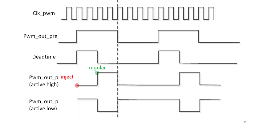
Figure 3-1: Adcmp-1
pwm_out_n: Based on the negative PWM wave generated after the dead time setting, the sampling time of the regular sequence is the rising edge of the pwm_out_n waveform, and the sampling time of the inject sequence is the starting point of the pwm cycle, as shown in the figure:
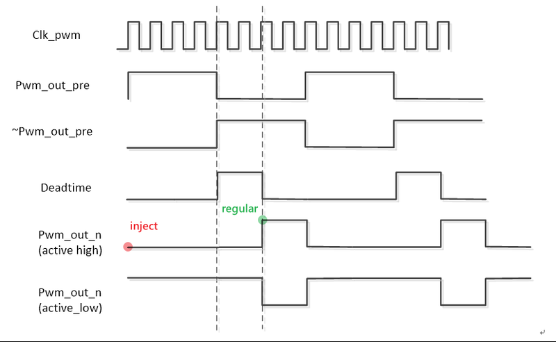
Figure 3-2: Adcmp-2
sw trigger: Notify the instruction to be sent to the register. After a command is triggered, the hardware performs a sampling.
external trigger: Specify the PIN pin. After the rising edge pulse is triggered after it is pulled low or high, the hardware performs a sampling.
freerun: Continuous sampling. If the sampling method is conversion, it supports sampling multiple data and outputting the average value. The sampling interval can also be set.
3.4. Sampling Method Description
adcmp sampling can choose two different methods: conversion and sequence.
conversion: Each trigger source will trigger the hardware to sample one channel.
- conversion + pwm_out_p trigger source: The rising edge of each pwm cycle triggers a sampling and collects data from one channel.
- conversion + sw trigger trigger source: Each time the sw trigger is executed, a sampling is triggered and data from one channel is collected.
- conversion + external trigger trigger source: Each time the external trigger is executed, a sampling is triggered and data from one channel is collected.
- conversion + freerun trigger source: After triggering once, continuous sampling is performed, supporting average sampling and setting the hardware sampling interval for each channel.
sequence: Each trigger source will trigger the hardware to sample all channels of the entire sequence.
- sequence + pwm_out_p trigger source: The rising edge of each pwm cycle triggers a sampling and collects data from all channels of the entire sequence
- sequence + sw trigger trigger source: Each time the sw trigger is executed, a sampling is triggered and data from all channels of the entire sequence is collected
- sequence + external trigger trigger source: Each time the external trigger is executed, a sampling is triggered and data from all channels of the entire sequence is collected
- sequence + freerun trigger source: After triggering once, continuous sampling is performed, and average sampling is not supported, nor is the hardware sampling interval for each channel supported
3.5. CALCULATION INSTRUCTION
The main function of SAR ADCMP is to convert analog signals into corresponding digital signals, that is, it can convert the input voltage into digital quantities and store them in registers, and calculate the input voltage through the formula.
Calculation formula: voltage = (register value / sampling accuracy 12-bit) * reference voltage.
That is, if the value read is 0x4B0, the voltage is 0x4B0/0xFFF *1.8 = about 0.53v.
4. HARDWARE CONNECTION INTRODUCTION
The corresponding relationship between different channels and PADs in different groups of SAR ADCMP:
| Group0 Channel Index | Pad Name |
|---|---|
| 0 | PAD_SAR_ADC0_00 |
| 1 | PAD_SAR_ADC0_01 |
| 2 | PAD_SAR_ADC0_02 |
| 3 | PAD_SAR_ADC0_03 |
| 4 | PAD_SAR_ADC0_04 |
| 5 | PAD_SAR_ADC0_05 |
| 6 | PAD_SAR_ADC0_06 |
| 7 | PAD_SAR_ADC0_07 |
| 8 | PAD_SAR_ADC0_08 |
| 9 | PAD_SAR_ADC0_09 |
| 10 | PAD_SAR_ADC0_10 |
| 11 | PAD_SAR_ADC0_11 |
| 12 | PAD_SAR_ADC0_12 |
| 13 | PAD_SAR_ADC0_13 |
| 14 | PAD_SAR_ADC0_14 |
| 15 | PAD_SAR_ADC0_11 |
| 16 | PAD_PM_GPIO0 |
| 17 | PAD_PM_GPIO1 |
| 18 | PAD_PM_GPIO3 |
| 19 | PAD_PM_GPIO6 |
| 20 | PAD_PM_ADC00_IN |
| 21 | PAD_PM_GPIO7 |
| Group1 Channel Index | Pad Name |
|---|---|
| 0 | PAD_PWM_OUT00 |
| 1 | PAD_PWM_OUT01 |
Taking PAD_SAR_ADC0_00 as an example, when connecting the hardware, check the schematic diagram to locate the pin position, and connect the external voltage to the pin PAD_SAR_ADC0_00, as shown in the following figure:
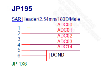
Figure 4-1: Adcmp-3
5. RISCV USAGE INTRODUCTION
5.1. Driver Path
sc/driver/sysdriver/saradc/os/adcmp_os.h
sc/driver/sysdriver/saradc/drv/pub/drv_adcmp.h
sc/driver/sysdriver/saradc/drv/src/drv_adcmp.c
sc/driver/sysdriver/saradc/drv/src/drv_adcmp_test.c
sc/driver/sysdriver/saradc/hal/chipname/src/hal_adcmp.c
sc/driver/sysdriver/saradc/hal/chipname/inc/hal_adcmp.h
sc/driver/sysdriver/saradc/hal/chipname/inc/hal_adcmp_cfg.h
5.2. CONFIG Configuration
The config file is located at mak/options_chipname_riscv_isw.mak, enable CONFIG_SARADC_SUPPORT.
# Feature_Name = [DRV] SARADC driver support
# Description = SARADC driver support
# Option_Selection = TRUE, FALSE
CONFIG_SARADC_SUPPORT = TRUE
5.3. SYSDESC Configuration
The chipname_xxx.sys file is used to describe the hardware attributes of peripherals. The attribute values contained in the peripheral node can be used to configure the peripherals, similar to the Linux device tree. The file is located in sc/driver/sysdriver/sysdesc/hal/chipname/pub.
<adcmp0>
    [reg_u32] 0x200AC00, 0x200AE00, 0x2003C00, 0x2204600, 0x2203E00;
    [interrupts_u32] INT_PM_FIQ_ADCMP;
    [camclk_u16] CAMCLK_pm_pwm_adc;
    [interrupts_en_u8] 0;
    [dma_en_u8] 0;
    [dma_count_u32] 50;
    [clk_level_u8] 0;
    [ref_vol_u32] 1800;
    [regular_method_u8] 0;
    [inject_method_u8] 0;
    [regular_ch_u8] 0, 1, 2, 3, 4, 5, 6, 7, 8, 9, 10, 11;
    [inject_ch_u8] 12, 13, 14, 15, 16, 17, 18, 19, 20, 21;
    [upper_bound_u16] 0xFFFF, 0xFFFF, 0xFFFF, 0xFFFF, 0xFFFF, 0xFFFF, 0xFFFF, 0xFFFF, 0xFFFF,   0xFFFF, 0xFFFF, 0xFFFF, 0xFFFF, 0xFFFF, 0xFFFF, 0xFFFF, 0xFFFF, 0xFFFF, 0xFFFF, 0xFFFF,0xFFFF, 0xFFFF;
    [lower_bound_u16] 0, 0, 0, 0, 0, 0, 0, 0, 0, 0, 0, 0, 0, 0, 0, 0, 0, 0, 0, 0, 0, 0;
    [status_u8] 0;

<adcmp1>
    [reg_u32] 0x2203600, 0x2203A00, 0x2200E00, 0x2204600, 0x2203E00;
    [interrupts_u32] INT_FIQ_ADCMP;
    [camclk_u16] CAMCLK_pwm_adc;
    [interrupts_en_u8] 0;
    [dma_en_u8] 0;
    [dma_count_u32] 50;
    [clk_level_u8] 3;
    [ref_vol_u32] 1800;
    [regular_method_u8] 0;
    [inject_method_u8] 0;
    [regular_ch_u8] 0, 1;
    [upper_bound_u16] 0xFFFF, 0xFFFF;
    [lower_bound_u16] 0, 0;
    [status_u8] 0;
| Attribute | Description | Setting Value | Remark |
|---|---|---|---|
| reg_u32 | Set the register bank address | Modification prohibited | |
| interrupts_u32 | Bind the interrupt number | INT_PM_FIQ_ADCMP & INT_FIQ_ADCMP | Modification prohibited |
| camclk_u16 | Set the clock source | CAMCLK_pm_pwm_adc & CAMCLK_pwm_adc | Modification prohibited |
| interrupts_en_u8 | Enable interrupt | 1: enable, 0: disable | Can be modified as needed |
| dma_en_u8 | Enable DMA | 1: enable, 0: disable, to use the DMA function, interrupts must be enabled | Can be modified as needed |
| dma_count_u32 | DMA sampling number | Must be an even number | Can be modified as needed |
| ref_vol_u32 | Set the reference voltage range | In mv, group0 can choose 1500, 1800, group1 can only be set to 1800 | Can be modified as needed |
| clk_level_u8 | Set the clock source | Switch the clock source to change the sampling time, group0 can choose 0->24M, 1->12M, group1 can choose 0->24M, 1->12M, 2->6M, 3->80M | Can be modified as needed |
| regular_method_u8 | Set the sampling method of the regular sequence | 0:conversion, 1:sequence | Can be modified as needed |
| inject_method_u8 | Set the sampling method of the inject sequence | 0:conversion, 1:sequence | Can be modified as needed |
| regular_ch_u8 | Set the ADC sampling channel of the regular sequence | Set up to 23 ADC channels, arranged from left to right in the sampling order | Can be modified as needed |
| inject_ch_u8 | Set the ADC sampling channel of the inject sequence | Set up to 12 ADC channels, arranged from left to right in the sampling order | Can be modified as needed |
| upper_bound_u16 | Set the upper threshold voltage | 0~0xFFFF | Can be modified as needed |
| lower_bound_u16 | Set the lower threshold voltage | 0~0xFFFF | Can be modified as needed |
| status | Whether to enable the driver | 1: enable, 0: disable | Can be modified as needed |
Taking the DMA sampling function as an example, assuming that the DTS configuration is as follows:
<adcmp0>
    ......
    [interrupts_u32] INT_PM_FIQ_ADCMP;
    [camclk_u16] CAMCLK_pm_pwm_adc;
    [interrupts_en_u8] 1;  //DMA function must enable interrupt
    [dma_en_u8] 1;        //Enable DMA
    [dma_count_u32] 200;  //Each time sampling is triggered, 200 ADC data will be collected continuously
    [clk_level_u8] 0;
    [ref_vol_u32] 1800;
    [regular_method_u8] 0;
    [inject_method_u8] 0;
    [regular_ch_u8] 0, 1, 2, 3, 4, 5;
    [inject_ch_u8] 12, 13, 14, 15;
    ......
The configuration that affects the DMA sampling results is as follows:
[clk_level_u8] 0:Sampling frequency = 24M / 16 = 1.5M hz,therefore, the sampling interval of each ADC data = 1000000000 / 1.5M = 667ns
[dma_count_u32] 200:200 ADC data are collected after each DMA trigger, so the total hardware sampling time after each DMA trigger is 667ns * 200 = 133400ns
[regular_ch_u8] 0, 1, 2, 3, 4, 5; [inject_ch_u8] 12, 13, 14, 15;:The 200 collected data include the ADC data of channel0, 1, 2, 3, 4, 5, 12, 13, 14, 15,
Since the inject sequence has a higher priority, the sampling results are arranged in the order of channel 12 -> channel 13 -> channel 14 -> channel 15 -> channel 0 -> channel 1 -> channel 2 -> channel 3 -> channel 4 -> channel 5....
<adcmp1>
    ......
    [interrupts_u32] INT_FIQ_ADCMP;
    [camclk_u16] CAMCLK_pwm_adc;
    [interrupts_en_u8] 1;  //DMA function must enable interrupt
    [dma_en_u8] 1;        //Enable DMA
    [dma_count_u32] 400;  //Each time sampling is triggered, 400 ADC data will be collected continuously
    [clk_level_u8] 3;
    [ref_vol_u32] 1800;
    [regular_method_u8] 1;
    [regular_ch_u8] 0, 1;
    ......
The configuration that affects the DMA sampling results is as follows:
[clk_level_u8] 3; [regular_method_u8] 1;:Sampling frequency = 80M / 16 = 5M hz(if regular-method = <0>, then sampling frequency = 80M / 15 = 5.33M hz),therefore, the sampling interval of each ADC data = 1000000000 / 5M = 200ns
[dma_count_u32] 400:400 ADC data are collected after each DMA trigger, so the total hardware sampling time after each DMA trigger is200ns * 400 = 80000ns
[regular_ch_u8] 0, 1:The 400 collected data include the ADC data of channel0 and channel 1,the sampling results are arranged in the order of channel 0 -> channel 1 -> channel 0 -> channel 1 -> ....
5.4. PADMUX Configuration
CONFIG Configuration: CONFIG_PADMUX_SUPPORT=TRUE
If the chipname_xxx.sys file is configured with the attribute <padmux>, then the PADMUX setting is directly configured here:
<padmux>
    [schematic_u32_u32_u32]
            //pm adc 22ch
            PAD_SAR_ADC0_00  PINMUX_FOR_PMADC0_MODE_1 MDRV_PUSE_PWMADC0,
            PAD_SAR_ADC0_01 PINMUX_FOR_PMADC1_MODE_1 MDRV_PUSE_PWMADC1,
            PAD_SAR_ADC0_02 PINMUX_FOR_PMADC2_MODE_1 MDRV_PUSE_PWMADC2,
            PAD_SAR_ADC0_03  PINMUX_FOR_PMADC3_MODE_1 MDRV_PUSE_PWMADC3,
            PAD_SAR_ADC0_04 PINMUX_FOR_PMADC4_MODE_1 MDRV_PUSE_PWMADC4,
            PAD_SAR_ADC0_05  PINMUX_FOR_PMADC5_MODE_1 MDRV_PUSE_PWMADC5,
            PAD_SAR_ADC0_06  PINMUX_FOR_PMADC6_MODE_1 MDRV_PUSE_PWMADC6,
            PAD_SAR_ADC0_07  PINMUX_FOR_PMADC7_MODE_1 MDRV_PUSE_PWMADC7,
            PAD_SAR_ADC0_08 PINMUX_FOR_PMADC8_MODE_1 MDRV_PUSE_PWMADC8,
            PAD_SAR_ADC0_09  PINMUX_FOR_PMADC9_MODE_1 MDRV_PUSE_PWMADC9,
            PAD_SAR_ADC0_10 PINMUX_FOR_PMADC10_MODE_1 MDRV_PUSE_PWMADC10,
            PAD_SAR_ADC0_11  PINMUX_FOR_PMADC11_MODE_1 MDRV_PUSE_PWMADC11,
            PAD_SAR_ADC0_12 PINMUX_FOR_PMADC12_MODE_1 MDRV_PUSE_PWMADC12,
            PAD_SAR_ADC0_13  PINMUX_FOR_PMADC13_MODE_1 MDRV_PUSE_PWMADC13,
            PAD_SAR_ADC0_14  PINMUX_FOR_PMADC14_MODE_1 MDRV_PUSE_PWMADC14,
            PAD_PM_GPIO0   PINMUX_FOR_PMADC15_MODE_1 MDRV_PUSE_PWMADC15,
            PAD_PM_GPIO1     PINMUX_FOR_PMADC16_MODE_1 MDRV_PUSE_PWMADC16,
            PAD_PM_GPIO2     PINMUX_FOR_PMADC17_MODE_1 MDRV_PUSE_PWMADC17,
            PAD_PM_GPIO3     PINMUX_FOR_PMADC18_MODE_1 MDRV_PUSE_PWMADC18,
            PAD_PM_GPIO6      PINMUX_FOR_PMADC19_MODE_1 MDRV_PUSE_PWMADC19,
            PAD_PM_ADC00_IN PINMUX_FOR_PMADC20_MODE_1 MDRV_PUSE_PWMADC20,
            PAD_PM_GPIO7     PINMUX_FOR_PMADC21_MODE_1 MDRV_PUSE_PWMADC21,
            PAD_PM_PWM0_OUT    PINMUX_FOR_PM_ADC_INT_MODE_2 MDRV_PUSE_PMPWMADC_INT,

            //non pm adc 2ch
            PAD_PWM_OUT00     PINMUX_FOR_ADC0_MODE_1 MDRV_PUSE_PWMADC22,
            PAD_PWM_OUT01     PINMUX_FOR_ADC1_MODE_1 MDRV_PUSE_PWMADC23,
            PAD_GPIOA_12 PINMUX_FOR_PWM_INT_MODE_1 MDRV_PUSE_PWMADC_INT,
            PAD_GPIOA_13 PINMUX_FOR_PWM_INT_MODE_1 MDRV_PUSE_PWMOUT_INT;
    [status_u8] 1;
Otherwise, enable the PADMUX driver and configure the pin multiplexing function in the chipname-xxx-padmux.c file, which is located in sc/driver/sysdriver/padmux/hal/chipname/src. You only need to add the following content to the corresponding schematic attribute:
pad_info_t schematic[] =
{
    //pm adc 22ch
    {PAD_SAR_ADC0_00  PINMUX_FOR_PMADC0_MODE_1 MDRV_PUSE_PWMADC0},
    {PAD_SAR_ADC0_01 PINMUX_FOR_PMADC1_MODE_1 MDRV_PUSE_PWMADC1},
    {PAD_SAR_ADC0_02 PINMUX_FOR_PMADC2_MODE_1 MDRV_PUSE_PWMADC2},
    {PAD_SAR_ADC0_03  PINMUX_FOR_PMADC3_MODE_1 MDRV_PUSE_PWMADC3},
    {PAD_SAR_ADC0_04 PINMUX_FOR_PMADC4_MODE_1 MDRV_PUSE_PWMADC4},
    {PAD_SAR_ADC0_05  PINMUX_FOR_PMADC5_MODE_1 MDRV_PUSE_PWMADC5},
    {PAD_SAR_ADC0_06  PINMUX_FOR_PMADC6_MODE_1 MDRV_PUSE_PWMADC6},
    {PAD_SAR_ADC0_07  PINMUX_FOR_PMADC7_MODE_1 MDRV_PUSE_PWMADC7},
    {PAD_SAR_ADC0_08 PINMUX_FOR_PMADC8_MODE_1 MDRV_PUSE_PWMADC8},
    {PAD_SAR_ADC0_09  PINMUX_FOR_PMADC9_MODE_1 MDRV_PUSE_PWMADC9},
    {PAD_SAR_ADC0_10 PINMUX_FOR_PMADC10_MODE_1 MDRV_PUSE_PWMADC10},
    {PAD_SAR_ADC0_11  PINMUX_FOR_PMADC11_MODE_1 MDRV_PUSE_PWMADC11},
    {PAD_SAR_ADC0_12 PINMUX_FOR_PMADC12_MODE_1 MDRV_PUSE_PWMADC12},
    {PAD_SAR_ADC0_13  PINMUX_FOR_PMADC13_MODE_1 MDRV_PUSE_PWMADC13},
    {PAD_SAR_ADC0_14  PINMUX_FOR_PMADC14_MODE_1 MDRV_PUSE_PWMADC14},
    {PAD_PM_GPIO0   PINMUX_FOR_PMADC15_MODE_1 MDRV_PUSE_PWMADC15},
    {PAD_PM_GPIO1     PINMUX_FOR_PMADC16_MODE_1 MDRV_PUSE_PWMADC16},
    {PAD_PM_GPIO2     PINMUX_FOR_PMADC17_MODE_1 MDRV_PUSE_PWMADC17},
    {PAD_PM_GPIO3     PINMUX_FOR_PMADC18_MODE_1 MDRV_PUSE_PWMADC18},
    {PAD_PM_GPIO6      PINMUX_FOR_PMADC19_MODE_1 MDRV_PUSE_PWMADC19},
    {PAD_PM_ADC00_IN PINMUX_FOR_PMADC20_MODE_1 MDRV_PUSE_PWMADC20},
    {PAD_PM_GPIO7     PINMUX_FOR_PMADC21_MODE_1 MDRV_PUSE_PWMADC21},
    {PAD_PM_PWM0_OUT    PINMUX_FOR_PM_ADC_INT_MODE_2 MDRV_PUSE_PMPWMADC_INT},

    //non pm adc 2ch
    {PAD_PWM_OUT00     PINMUX_FOR_ADC0_MODE_1 MDRV_PUSE_PWMADC22},
    {PAD_PWM_OUT01     PINMUX_FOR_ADC1_MODE_1 MDRV_PUSE_PWMADC23},
    {PAD_GPIOA_12 PINMUX_FOR_PWM_INT_MODE_1 MDRV_PUSE_PWMADC_INT},
    {PAD_GPIOA_13 PINMUX_FOR_PWM_INT_MODE_1 MDRV_PUSE_PWMOUT_INT},
};
The first column is the pin index number, which can be queried in sc/drivers/sysdriver/gpio/hal/chipname/pub/gpio.h;
The second column is the mode definition, which can be queried in sc/drivers/sysdriver/gpio/hal/chipname/pub/padmux.h;
The third column is the index name of the pin and matching mode, which can be queried in sc/drivers/sysdriver/padmux/drv/pub/drv_puse.h.
5.5. Sample Code
The demo source code is located at sc/driver/sysdriver/saradc/drv/src/drv_adcmp_test.c.
Note the calling order of dma sampling:drv_adcmp_set_config()->drv_adcmp_register_callback()->drv_adcmp_dma_sample_trigger()->call drv_adcmp_dma_sample_data() in the callback function
6. API Reference
The header file is located in sc/driver/sysdriver/saradc/drv/pub/drv_adcmp.h.
struct adcmp_bound
{
    u8  channel;     //Specify the adc channel
    u8  bound_en;    //Enable the threshold monitoring function
    u16 lower_bd;    //The Lower threshold
    u16 upper_bd;    //The upper threshold
};

struct adcmp_config
{
    u8  inje_en;     //Enable the inject sequence sampling function
    u8  inje_mod;    //The inject sequence sampling trigger mode
    u8  regu_en;     //Enable the regular sequence sampling function
    u8  regu_mod;    //The regular sequence sampling trigger mode
    u8  avg_cnt;     //Number of samples to obtain the average value during freerun
    u32 p_delay;     //The delay time of pwm out p trigger during inject sampling
    u32 n_delay;     //The delay time of pwm out n trigger during inject sampling
    u16 sample_time; //The extended sampling interval during freerun(only supported in conversion method). If sample time = N, the final sampling interval = basic sampling time + extended sampling time = ( 1 / (clock source / 16)) + (N / (clock source / 4))
};

typedef s32 (*adcmp_cb_t)(u8 group);

int drv_adcmp_get_ref_vol(u8 group, u32 *voltage);
int drv_adcmp_set_bound(struct adcmp_bound *adcmp_bd, u8 group);
int drv_adcmp_set_config(struct adcmp_config *adcmp_cfg, u8 group);
int drv_adcmp_get_config(struct adcmp_config *adcmp_cfg, u8 group);
int int drv_adcmp_direct_read_ch(u8 group, u8 channel, u16 *value)(u8 group, u8 channel, u16 *value);
int drv_adcmp_direct_read_seq(u8 group, u8 linear_map, u16 *value);
int drv_adcmp_sample_channel(u8 group, u8 channel, u16 *value);
int drv_adcmp_sample_sequence(u8 group, u16 *value);
int drv_adcmp_sample_seq_linear_map(u8 group, u16 *value);
int drv_adcmp_dma_sample_trigger(u8 group);
int drv_adcmp_dma_sample_stop(u8 group);
int drv_adcmp_dma_sample_data(u8 group, u16 *value);
int drv_adcmp_register_callback(u8 group, adcmp_cb_t cb_t);
int drv_adcmp_unregister_callback(u8 group, adcmp_cb_t cb_t);
| API Name | Function |
|---|---|
| drv_adcmp_get_ref_vol | Get the current reference voltage |
| drv_adcmp_set_bound | Set the threshold of the specified channel |
| drv_adcmp_set_config | Set sampling attributes |
| drv_adcmp_get_config | Get sampling attributes |
| drv_adcmp_direct_read_ch | Directly obtain the external input voltage digital value of a specified single channel, without guaranteeing real-time performance |
| drv_adcmp_direct_read_seq | When DMA is not enabled, the external input voltage digital value of all channels of the regular sequence is directly obtained, and real-time performance is not guaranteed. |
| drv_adcmp_sample_channel | Get the external input voltage digital quantity of a specified single channel |
| drv_adcmp_sample_sequence | When dma is disabled, get the external input voltage digital quantity of all channels specified by Sysdesc |
| drv_adcmp_sample_seq_linear_map | When dma is disabled, get the external input voltage digital value of all channels specified by sysdesc and linearly map channels and data |
| drv_adcmp_dma_sample_trigger | Trigger the sampling function under dma mode |
| drv_adcmp_dma_sample_stop | Stop the sampling function under dma mode |
| drv_adcmp_dma_sample_data | Get the sampling data under dma mode |
| drv_adcmp_register_callback | Register the callback function of the specified group |
| drv_adcmp_unregister_callback | Release the callback function of the specified group and the memory applied during registration |
6.1. drv_adcmp_set_bound
-
Purpose
Set the threshold range of the adcmp specified channel.
-
Syntax
int drv_adcmp_set_bound(struct adcmp_bound *adcmp_bd, u8 group)
-
Parameter
Parameter name Description adcmp_bd Used to enable and configure the upper and lower thresholds of the adcmp specified channel group Specify the adcmp group -
Return value
Result Description Success Return 0 Failure Return negative numbers
6.2. drv_adcmp_set_config
-
Purpose
Set the sampling attributes of adcmp.
-
Syntax
int drv_adcmp_set_config(struct adcmp_config *adcmp_cfg, u8 group)
-
Parameter
Parameter name Description adcmp_cfg Configure the sampling attributes of adcmp group Specify the adcmp group -
Return value
Result Description Success Return 0 Failure Return negative numbers
6.3. drv_adcmp_get_config
-
Purpose
Get the sampling attributes of adcmp to prevent other attributes from being changed when updating parameters.
-
Syntax
drv_adcmp_get_config(struct adcmp_config *adcmp_cfg, u8 group)
-
Parameter
Parameter name Description adcmp_cfg Get the sampling attributes of the current adcmp group Specify the adcmp group -
Return value
Result Description Success Return 0 Failure Return negative numbers
6.4. drv_adcmp_sample_channel
-
Purpose
Get the external input voltage digital quantity of a specified single channel.
-
Syntax
int drv_adcmp_sample_channel(u8 group, u8 channel, u16 *value)
-
Parameter
Parameter name Description group Specify the adcmp group channel Specify the channel. Note that it must be a member of the attributes regular_ch_u8andinject_ch_u8in sysdescvalue Get the pointer of the sampling data -
Return value
Result Description Success Return 0 Failure Return negative numbers
6.5. drv_adcmp_sample_sequence
-
Purpose
When dma is disabled, get the external input voltage digital quantity of all channels specified by sysdesc.
-
Syntax
int drv_adcmp_sample_sequence(u8 group, u16 *value)
-
Parameter
Parameter name Description group Specify the adcmp group value Get the pointer of the sampling data, first get the sampling value of the channel specified by inject_ch_u8, then get the sampling value of the channel specified byregular_ch_u8 -
Return Value
Result Description Success Return 0 Failure Return negative numbers
6.6. drv_adcmp_dma_sample_trigger
-
Purpose
Trigger the sampling function under dma mode.
-
Syntax
int drv_adcmp_dma_sample_trigger(u8 group)
-
Parameter
Parameter name Description group Specify the adcmp group -
Return Value
Result Description Success Return 0 Failure Return negative numbers
6.7. drv_adcmp_dma_sample_stop
-
Purpose
Stop the sampling function under dma mode.
-
Syntax
int drv_adcmp_dma_sample_stop(u8 group)
-
Parameter
Parameter name Description group Specify the adcmp group -
Return Value
Result Description Success Return 0 Failure Return negative numbers
6.8. drv_adcmp_dma_sample_data
-
Purpose
Get the sampling data under dma mode. Note that function
drv_adcmp_dma_sample_triggermust be called before each refresh of the sampling results. -
Syntax
int drv_adcmp_dma_sample_data(u8 group, u16 *value)
-
Parameter
Parameter name Description group Specify the adcmp group value Get the pointer of sampling data, first get the sampling value of the channel specified by inject-ch, then get the sampling value of the channel specified byregular-ch -
Return Value
Result Description Success Return 0 Failure Return negative numbers
6.9. drv_adcmp_register_callback
-
Purpose
Register the callback function of the specified group. When dma sampling is completed, you can call
drv_adcmp_dma_sample_datain the callback function to get the sampling data. -
Syntax
int drv_adcmp_register_callback(u8 group, adcmp_cb_t cb_t)
-
Parameter
Parameter name Description group Specify the adcmp group cb_t Function pointer -
Return Value
Result Description Success Return 0 Failure Return negative numbers
6.10. drv_adcmp_unregister_callback
-
Purpose
Release the callback function of the specified group and the memory applied during registration
-
Syntax
int drv_adcmp_unregister_callback(u8 group, adcmp_cb_t cb_t)
-
Parameter
Parameter name Description group Specify the adcmp group cb_t Function pointer -
Return Value
Result Description Success Return 0 Failure Return negative numbers
6.11. drv_adcmp_get_ref_vol
-
Purpose
Get the current reference voltage
-
Syntax
int drv_adcmp_get_ref_vol(u8 group, u32 *voltage)
-
Parameter
Parameter name Description group Specify the adcmp group voltage Reference voltage, in mV -
Return Value
Result Description Success Return 0 Failure Return negative numbers
6.12. drv_adcmp_direct_read_ch
-
Purpose
Directly obtain the external input voltage digital value of a specified single channel. The difference from
drv_adcmp_sample_channelis that the result obtained by direct read does not guarantee real-time performance. It only supports channels in regular sequences, and the trigger source does not support sw trigger and external trigger.In terms of hardware, the channels of the regular sequence will be polled and sampled in a predetermined order. Using
drv_adcmp_sample_channelwill ensure that it is the sampling result of the current cycle.drv_adcmp_direct_read_chmay be the sampling result of the previous cycle, the current cycle, or the next cycle (one sampling cycle = number of regular sequence channels * (1 / sampling frequency), excluding the sampling time required for inject sequence preemption)A common scenario is when using DMA to collect a large amount of data. You can obtain the data of a certain channel before the DMA sampling ends.
-
Syntax
int drv_adcmp_direct_read_ch(u8 group, u8 channel, u16 *value)
-
Parameter
Parameter name Description group Specify the adcmp group channel Specifies the channel, which must be a member of the attribute regular_ch_u8in sysdescvalue Get the pointer of the sampling data -
Return Value
Result Description Success Return 0 Failure Return negative numbers -
Notes
Before the first use or after each call to
drv_adcmp_set_config, you need to calldrv_adcmp_sample_channelordrv_adcmp_dma_sample_triggerto trigger sampling;If
drv_adcmp_dma_sample_triggeris used,drv_adcmp_direct_read_chcan only obtain channel data during DMA sampling. When DMA sampling is completed, the data obtained bydrv_adcmp_direct_read_chwill not be updated. At this time, calldrv_adcmp_sample_channelto restore.
6.13. drv_adcmp_direct_read_seq
-
Purpose
Directly obtain the external input voltage digital value of a specified single channel. The difference from
drv_adcmp_sample_seqis that the result obtained by direct read does not guarantee real-time performance. It only supports channels in regular sequences, and the trigger source does not support sw trigger and external trigger.In terms of hardware, the channels of the regular sequence will be polled and sampled in a predetermined order. Using
drv_adcmp_sample_sequencewill ensure that it is the sampling result of the current cycle.drv_adcmp_direct_read_seqmay be the sampling result of the previous cycle, the current cycle, or the next cycle (one sampling cycle = number of regular sequence channels * (1 / sampling frequency), excluding the sampling time required for inject sequence preemption)A common scenario is when using DMA to collect a large amount of data. You can obtain the data of all channels in the entire sequence before the DMA sampling ends.
-
Syntax
int drv_adcmp_direct_read_seq(u8 group, u8 linear_map, u16 *value)
-
Parameter
Parameter name Description group Specify the adcmp group linear_map 0: value data is sorted according to the order defined by regular_ch_u8in sysdesc, 1: value data is sorted from small to large according to channel index, for example, value[0]=channel 0 adc datavalue Get the pointer of the sampling result, get the sampling values of all channels in regular_ch_u8 -
Return Value
Result Description Success Return 0 Failure Return negative numbers -
Notes
Before the first use or after each call to
drv_adcmp_set_config, you need to calldrv_adcmp_sample_sequenceordrv_adcmp_dma_sample_triggerto trigger sampling;If
drv_adcmp_dma_sample_triggeris used,drv_adcmp_direct_read_seqcan only obtain channel data during DMA sampling. When DMA sampling is completed, the data obtained bydrv_adcmp_direct_read_seqwill not be updated. At this time, calldrv_adcmp_sample_sequenceto restore
6.14. drv_adcmp_sample_seq_linear_map
-
Purpose
When dma is disabled, get the external input voltage digital value of all channels specified by sysdesc and linearly map channels and data.
-
Syntax
int drv_adcmp_sample_seq_linear_map(u8 group, u16 *value)
-
Parameter
Parameter name Description group Specify the adcmp group value Get the pointer of the sampling result. The data of value is sorted from small to large according to the channel index, for example, value[0] = channel 0 adc data, value[1] = channel 1 adc data -
Return Value
Result Description Success Return 0 Failure Return negative numbers
7. FAQ
Q1: SAR ADCMP Interface Does Not Exist
-
Check if the
status_u8of the sysdesc adcmp node is1 -
Check if the config is configured, see [5.2. CONFIG Configuration]
Q2: SAR ADCMP Sampling Results Do Not Change Synchronously with External Voltage
-
Set the pin to GPIO mode to test output high/low. If it cannot be pulled high or low, it may be a hardware problem.
-
Check whether the sampling trigger mode is ready. For example, pwm out p needs to configure pwm dead time and enable it. The external trigger needs the level to change to trigger the rising edge. In particular, if the trigger mode of the inject sequence is not enabled, the regular sequence cannot be sampled.
Q3: SAR ADCMPADCMP sampling result can only change in multiples of 256
When the input voltage of the PIN pin corresponding to a certain ADC channel is greater than the reference voltage, the sampling of the previous channel will be disturbed and the sampling result can only be a multiple of 256.
<adcmp0>
    [reg_u32] 0x200AC00, 0x200AE00, 0x2003C00, 0x2204600, 0x2203E00;
    [interrupts_u32] INT_PM_FIQ_ADCMP;
    [camclk_u16] CAMCLK_pm_pwm_adc;
    [interrupts_en_u8] 0;
    [dma_en_u8] 0;
    [dma_count_u32] 50;
    [clk_level_u8] 0;
    [ref_vol_u32] 1800;
    [regular_method_u8] 0;
    [inject_method_u8] 0;
    [regular_ch_u8] 0 1 2 8 3 9 4 5 6 7 10 11 12 13 14 15 16 17 18 19 20 21;
    [upper_bound_u16] 0xFFFF, 0xFFFF, 0xFFFF, 0xFFFF, 0xFFFF, 0xFFFF, 0xFFFF, 0xFFFF, 0xFFFF,   0xFFFF, 0xFFFF, 0xFFFF, 0xFFFF, 0xFFFF, 0xFFFF, 0xFFFF, 0xFFFF, 0xFFFF, 0xFFFF, 0xFFFF,0xFFFF, 0xFFFF;
    [lower_bound_u16] 0, 0, 0, 0, 0, 0, 0, 0, 0, 0, 0, 0, 0, 0, 0, 0, 0, 0, 0, 0, 0, 0;
    [status_u8] 1;
For example, in the above configuration, [ref_vol_u32] is 1.8V. If the input voltage of channel 8 and channel 9 is greater than 1.8V, the sampling results of channel 2 and channel 3 will be disturbed and can only be a multiple of 256.
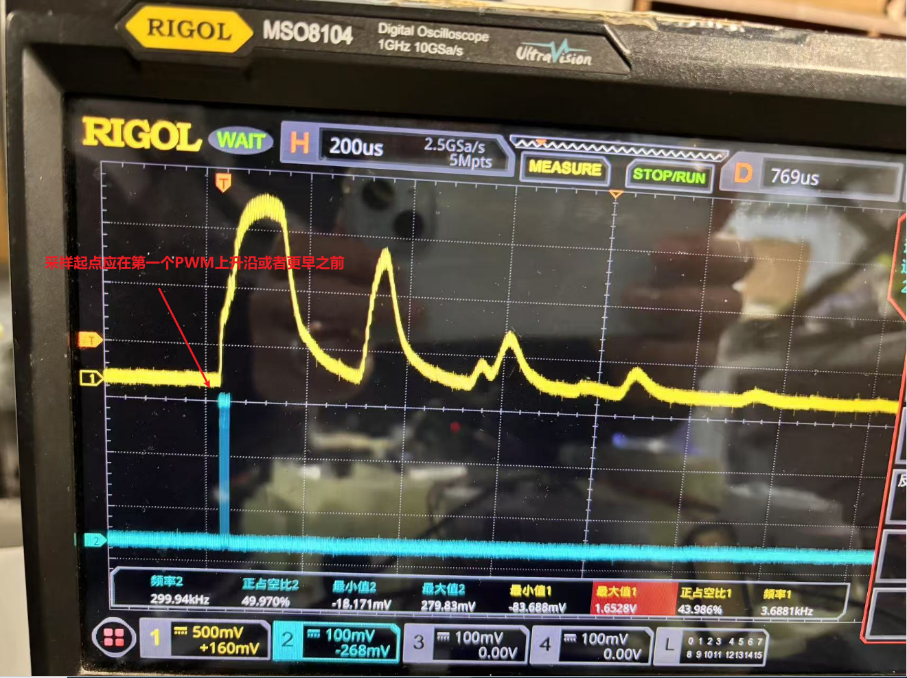
Q4: SAR ADCMP DMA sampling fails to obtain valid data in the ultrasonic scene
the application scenario is that the voltage (yellow) changes only after the PWM waveform (blue) is output.
If there is no error, it is just that the sampling data does not meet expectations. You need to check whether the DMA sampling timing matches the voltage change timing.
If adcmp0 is used at this time, the trigger mode of pwm_out (0~11) can be selected, and the sampling start point is the rising edge of the first PWM waveform, which can ensure that all ADC data are sampled synchronously.
If adcmp1 is used at this time, since there is no trigger mode of pwm_out, you can choose to trigger sampling first, and then control the output PWM waveform, and control the total sampling time according to the sampling count, and you can also sample all ADC data.