ADCMP USER GUIDE
REVISION HISTORY
| Revision No. | Description |
Date |
|---|---|---|
| 1.0 | 09/06/2024 | |
| 1.1 | 04/10/2025 | |
| 1.2 | 05/15/2025 |
1. OVERVIEW
The Successive Approximation ADC uses a feedback comparison circuit structure. The implementation method is briefly summarized as follows: take a digital quantity and add it to the DAC to get a corresponding output analog voltage. Compare this analog voltage with the input analog voltage signal. If the two are not equal, adjust the digital quantity until the two analog voltages are equal. The final digital quantity is the desired conversion result.
2. KEYWORD DESCRIPTION
-
ADCLP
Analog-to-digital converter Low Precision, low-precision (10-bit) analog-to-digital converter.
-
ADCMP
Analog-to-digital converter Medium Precision, medium-precision (12bit) analog-to-digital converter.
-
Regular/inject
Different ADC channels can be added to the regular sequence or the inject sequence in different sampling orders. The sampling priority of the inject sequence is higher than that of the regular sequence.
-
Reference voltage
The reference voltage used for analog-to-digital conversion calculations, which is also the maximum range, if the reference voltage is set to 1.8v, when the external input voltage is >=1.8v, the digital value reaches the maximum value of 4095.
3. FUNCTION DESCRIPTION
SAR ADCMP sampling precision is 12-bit, and the hardware design is divided into 2 groups. Group0 and group1 are used to distinguish below, where group0 belongs to pm domain and group1 belongs to nonpm domain.
3.1. Group0 Function Description
-
Supports 22 ADC channels sampling, and can use regular sequence and inject sequence at the same time.
-
The regular sequence can be configured with up to 23 ADC channels (group0 has a total of 22 channels, and the extra channel can be selected as unconfigured or configured as a duplicate channel), and the inject sequence can be configured with up to 12 ADC channels (the sampling priority is greater than the regular sequence, but it is not recommended to overlap the channels of the regular sequence in non-DMA mode).
-
Regular sequence supports 15 sampling trigger modes, and inject sequence supports 14 sampling trigger modes.
-
Sampling frequency = clock source / 16, optional clock sources are 24M and 12M.(The inverse of the sampling frequency is the time required to acquire one data point on the hardware)
-
Supports 1.5V, 1.8V, a total of 2 gear reference voltages.
3.2. Group1 Function Description
-
Supports 2 ADC channels sampling, and cannot use regular sequence and inject sequence at the same time, only one can be selected.
-
The regular sequence can be configured with a maximum of 23 adc channels (group1 has a total of 2 channels, and the remaining 21 channels can be configured or unconfigured as repeated channels), and the inject sequence can be configured with a maximum of 12 adc channels (the remaining 10 channels can be configured as unconfigured or repeated channels, but they cannot be used simultaneously with the regular sequence).
-
Regular sequence supports 3 sampling trigger modes, and inject sequence supports 2 sampling trigger modes.
-
Sampling frequency = clock source / N, the optional clock sources are 80M, 24M, 12M, 6M; when the sampling method is conversion, N=15; when the sampling method is sequence, N=16.(The inverse of the sampling frequency is the time required to acquire one data point on the hardware.)
-
Supports 1.8V reference voltage.
3.3. Trigger Mode Description
Summary of trigger modes supported by adcmp:
| NO. | trigger-modes | group0-regular | group0-inject | group1-regular | group1-inject |
|---|---|---|---|---|---|
| 0 | pwm12_out_p | ||||
| 1 | pwm12_out_n | ||||
| 2 | pwm13_out_p | ||||
| 3 | pwm13_out_n | ||||
| 4 | pwm14_out_p | ||||
| 5 | pwm14_out_n | ||||
| 6 | pwm15_out_p | ||||
| 7 | pwm15_out_n | ||||
| 8 | pwm16_out_p | ||||
| 9 | pwm16_out_n | ||||
| 10 | pwm17_out_p | ||||
| 11 | pwm17_out_n | ||||
| 12 | sw trigger | ||||
| 13 | external trigger | ||||
| 14 | freerun |
pwm_out_p: Based on the positive PWM wave generated after the dead time setting, the sampling time of the regular sequence is the rising edge of the pwm_out_p waveform, and the sampling time of the inject sequence is the starting point of the pwm cycle, as shown in the figure:
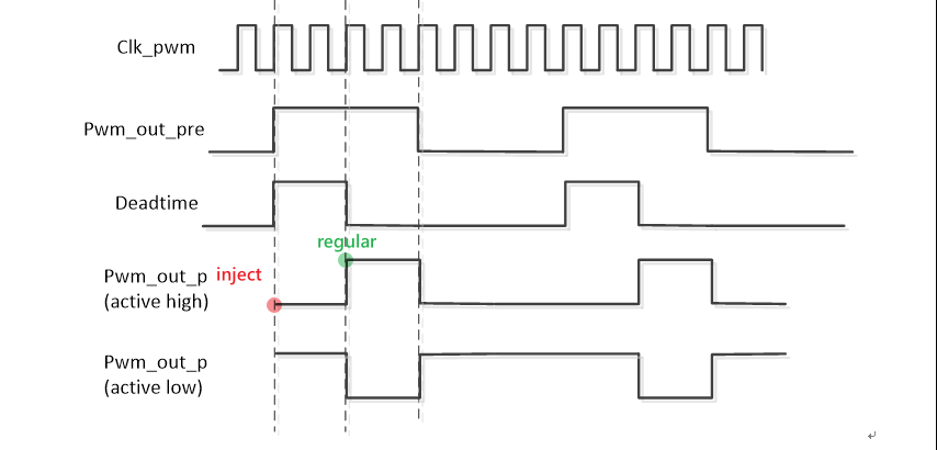
Figure 3-1: Adcmp-1
pwm_out_n: Based on the negative PWM wave generated after the dead time setting, the sampling time of the regular sequence is the rising edge of the pwm_out_n waveform, and the sampling time of the inject sequence is the starting point of the pwm cycle, as shown in the figure:
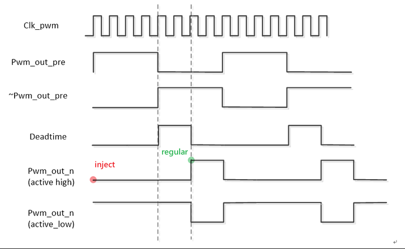
Figure 3-2: Adcmp-2
sw trigger: Notify the instruction to be sent to the register. After a command is triggered, the hardware performs a sampling.
external trigger: Specify the PIN pin. After the rising edge pulse is triggered after it is pulled low or high, the hardware performs a sampling.
freerun: Continuous sampling. If the sampling method is conversion, it supports sampling multiple data and outputting the average value. The sampling interval can also be set.
3.4. Sampling Method Description
adcmp sampling can choose two different methods: conversion and sequence.
conversion: Each trigger source will trigger the hardware to sample one channel.
- conversion + pwm_out_p trigger source: The rising edge of each pwm cycle triggers a sampling and collects data from one channel.
- conversion + sw trigger trigger source: Each time the sw trigger is executed, a sampling is triggered and data from one channel is collected.
- conversion + external trigger trigger source: Each time the external trigger is executed, a sampling is triggered and data from one channel is collected.
- conversion + freerun trigger source: After triggering once, continuous sampling is performed, supporting average sampling and setting the hardware sampling interval for each channel.
sequence: Each trigger source will trigger the hardware to sample all channels of the entire sequence.
- sequence + pwm_out_p trigger source: The rising edge of each pwm cycle triggers a sampling and collects data from all channels of the entire sequence
- sequence + sw trigger trigger source: Each time the sw trigger is executed, a sampling is triggered and data from all channels of the entire sequence is collected
- sequence + external trigger trigger source: Each time the external trigger is executed, a sampling is triggered and data from all channels of the entire sequence is collected
- sequence + freerun trigger source: After triggering once, continuous sampling is performed, and average sampling is not supported, nor is the hardware sampling interval for each channel supported
3.5. CALCULATION INSTRUCTION
The main function of SAR ADCMP is to convert analog signals into corresponding digital signals, that is, it can convert the input voltage into digital quantities and store them in registers, and calculate the input voltage through the formula.
Calculation formula: voltage = (register value / sampling accuracy 12-bit) * reference voltage.
That is, if the value read is 0x4B0, the voltage is 0x4B0/0xFFF *1.8 = about 0.53v.
4. HARDWARE CONNECTION INTRODUCTION
The corresponding relationship between different channels and PADs in different groups of SAR ADCMP:
| Group0 Channel Index | Pad Name |
|---|---|
| 0 | PAD_SAR_ADC0_00 |
| 1 | PAD_SAR_ADC0_01 |
| 2 | PAD_SAR_ADC0_02 |
| 3 | PAD_SAR_ADC0_03 |
| 4 | PAD_SAR_ADC0_04 |
| 5 | PAD_SAR_ADC0_05 |
| 6 | PAD_SAR_ADC0_06 |
| 7 | PAD_SAR_ADC0_07 |
| 8 | PAD_SAR_ADC0_08 |
| 9 | PAD_SAR_ADC0_09 |
| 10 | PAD_SAR_ADC0_10 |
| 11 | PAD_SAR_ADC0_11 |
| 12 | PAD_SAR_ADC0_12 |
| 13 | PAD_SAR_ADC0_13 |
| 14 | PAD_SAR_ADC0_14 |
| 15 | PAD_SAR_ADC0_11 |
| 16 | PAD_PM_GPIO0 |
| 17 | PAD_PM_GPIO1 |
| 18 | PAD_PM_GPIO3 |
| 19 | PAD_PM_GPIO6 |
| 20 | PAD_PM_ADC00_IN |
| 21 | PAD_PM_GPIO7 |
| Group1 Channel Index | Pad Name |
|---|---|
| 0 | PAD_PWM_OUT00 |
| 1 | PAD_PWM_OUT01 |
Taking PAD_SAR_ADC0_00 as an example, when connecting the hardware, check the schematic diagram to locate the pin position, and connect the external voltage to the pin PAD_SAR_ADC0_00, as shown in the following figure:
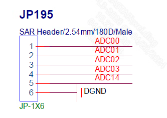
Figure 4-1: Adcmp-3
5. UBOOT USAGE INTRODUCTION
5.1. Uboot Config Configuration
Check Kconfig to see that supporting ADCMP requires configuring CONFIG_SSTAR_ADCMLP, CONFIG_ADC, CONFIG_CMD_ADC. To enable CONFIG_CMD_ADC, you need to configure DM_REGULATOR first.
-
Configure CONFIG_SSTAR_ADCMP

Figure 5-1: Adcmp-7
-
Configure CONFIG_ADC

Figure 5-2: Adcmp-4
-
Configure DM_REGULATOR
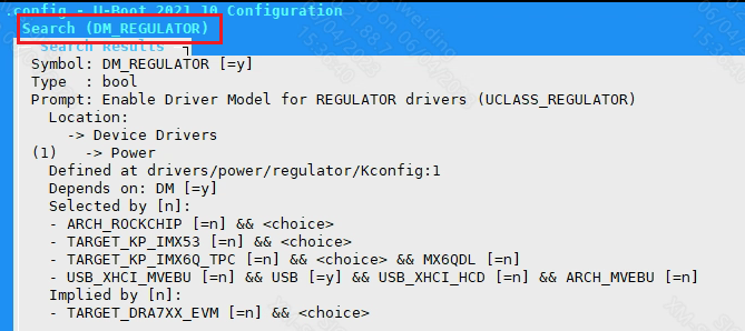
Figure 5-3: Adcmp-6
-
Configure CONFIG_CMD_ADC

Figure 5-4: Adcmp-5
5.2. DTS Configuration
The DTS configuration of SAR ADCMP only needs to configure the following information in chipname.dtsi:
adcmp0: adcmp0 {
    compatible = "sstar,adcmp";
    reg = <0x1F00AC00 0x200>, <0x1F00AE00 0x200>, <0x1F003C00 0x200>,<0x1F204600 0x200>, <0x1F203E00 0x200>;
    group = <0>;
    //1500mv 1800mv
    ref-voltage = <1800>;
    //24M 12M
    clock-freq = <24000000>;
    regular-method = <0>;
    inject-method = <0>;
    trigger-source = <12 12>; //sw trigger
    regular-ch = <0 1 2 3 4 5 6 7 8 9 10 11>;
    inject-ch = <12 13 14 15 16 17 18 19 20 21>;
    status = "okay";
};

adcmp1: adcmp1 {
    compatible = "sstar,adcmp";
    reg = <0x1F203600 0x200>, <0x1F203A00 0x200>, <0x1F200E00 0x200>, <0x1F204600 0x200>, <0x1F203E00 0x200>;
    group = <1>;
    //1800mv
    ref-voltage = <1800>;
    //24M 12M 6M 80M
    clock-freq = <80000000>;
    regular-method = <0>;
    inject-method = <0>;
    trigger-source = <12>; //sw trigger
    regular-ch = <0 1>;
    status = "okay";
};
SAR ADCMP DTS configuration description:
| Attribute | Description | Setting Value | Remark |
|---|---|---|---|
| compatible | Match the driver for registration | "sstar,adcmp" | Modification prohibited |
| reg | Set the register bank address | Modification prohibited | |
| group | Set the group | 0, 1 | Modification prohibited |
| ref-voltage | Set the reference voltage range | In mv, group0 can choose 1500 and 1800, group1 can only be set to 1800 | Can be modified as needed |
| clock-freq | Set the clock frequency | Switch the clock frequency to change the sampling time. Group 0 can choose 24M and 12M, group 1 can choose 024M, 12M, 6M and 80M | Can be modified as needed |
| regular-method | Set the sampling method of the regular sequence | 0:conversion, 1:sequence | Can be modified as needed |
| inject-method | Set the sampling method of the inject sequence | 0:conversion, 1:sequence | Can be modified as needed |
| trigger-source | Set the sampling trigger source of regular sequence and inject sequence | For parameters, please refer to Trigger Mode Description | Modification prohibited |
| regular-ch | Set ADC sampling channels of the regular sequence | Set up to 23 ADC channels, arranged from left to right in the sampling order | Can be modified as needed |
| inject-ch | Set ADC sampling channels of the inject sequence | Set up to 12 ADC channels, arranged from left to right in the sampling order | Can be modified as needed |
| status | Select whether to enable the driver | "okay" or "disable" | Can be modified as needed |
5.3. Uboot cmd Parameter Description and Use Case
-
In command lines, input adc.
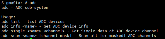
Figure 5-5: Adcmp-8
-
adc list -> check whether sar adcmp is bound.
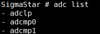
Figure 5-6: Adcmp-9
-
adc info adcmp0 -> view the number of channels and data precision supported by adcmp0.
As shown below, the number of channels supported by adcmp0 is 22 (note that the mask is 0x3fffff), and the maximum data value is 0xfff.

Figure 5-7: Adcmp-10
-
adc single adcmp0 [channel] -> view the data of a specific channel of adcmp0
As shown in the figure below, the value of channel 0 is 1252.
According to the formula: voltage = (data / 0xfff) * reference voltage.
At this time, the voltage is 1252 / 4095 * 1.8 V = 0.550V.

Figure 5-8: Adcmp-11
-
adc scan adcmp0 [channel mask] -> view the data of multiple channels.
adc scan adcmp0: view the data of all channels.
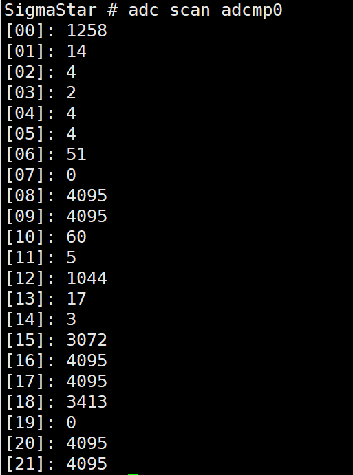
Figure 5-9: Adcmp-12
adc scan adcmp0 0x3: view the data of channel 0 and channel 1 of adcmp0.
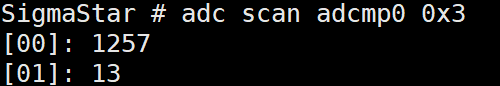
Figure 5-10: Adcmp-13
6. KERNEL USAGE INTRODUCTION
6.1. Kernel Config Configuration
SAR ADCMP associated driver module Config:
-
CONFIG_IIO
-
CONFIG_IRQ_WORK
-
CONFIG_IIO_BUFFER
-
CONFIG_IIO_TRIGGER
-
CONFIG_IIO_TRIGGERED_BUFFER
SAR ADCMP driver enable requires the following configuration:
Device Drivers --->

    [*] Sstar SoC platform drivers --->

        <*> Sstar ADCMP driver
6.2. DTS Configuration
The DTS configuration of SAR ADCMP only needs to configure the following information in chipname.dtsi:
adcmp0: adcmp@1f00ac00 {
    compatible = "sstar,adcmp";
    reg = <0x0 0x1F00AC00 0x0 0x200>, <0x0 0x1F00AE00 0x0 0x200>, <0x0 0x1F003C00 0x0 0x200>, <0x0 0x1F204600 0x0 0x200>, <0x0 0x1F203E00 0x0 0x200>;
    clocks = <&CLK_pm_pwm_adc>;
    interrupt-parent = <&sstar_pm_main_intc>;
    interrupts = <INT_PMSLEEP_FIQ_ADC>;
    interrupts-enable;
    group = <0>;
    //dma-enable;
    //dma-count = <50>;
    ref-voltage = <1800>;//1.5V 1.8V
    //0:24M 1:12M
    clk-select = <0>;
    regular-method = <0>;
    inject-method = <0>;
    regular-ch = <0 1 2 3 4 5 6 7 8 9 10 11>;
    inject-ch = <12 13 14 15 16 17 18 19 20 21>;
    upper-bound = <0xFFFF 0xFFFF 0xFFFF 0xFFFF 0xFFFF 0xFFFF 0xFFFF 0xFFFF 0xFFFF 0xFFFF 0xFFFF 0xFFFF
                    0xFFFF 0xFFFF 0xFFFF 0xFFFF 0xFFFF 0xFFFF 0xFFFF 0xFFFF 0xFFFF 0xFFFF>;
    lower-bound = <0 0 0 0 0 0 0 0 0 0 0 0 0 0 0 0 0 0 0 0 0 0>;
    status = "okay";
};

adcmp1: adcmp@1f203600 {
    compatible = "sstar,adcmp";
    reg = <0x0 0x1F203600 0x0 0x200>, <0x0 0x1F203A00 0x0 0x200>, <0x0 0x1F200E00 0x0 0x200>, <0x0 0x1F204600 0x0 0x200>, <0x0 0x1F203E00 0x0 0x200>;
    clocks = <&CLK_pwm_adc>;
    interrupts = <GIC_SPI INT_FIQ_ADCMP IRQ_TYPE_LEVEL_HIGH>;
    interrupts-enable;
    group = <1>;
    //dma-enable;
    //dma-count = <50>;
    ref-voltage = <1800>; //only support 1.8V
    //0->24M, 1->12M, 2->6M, 3->80M
    clk-select = <3>;
    regular-method = <0>;
    inject-method = <0>;
    regular-ch = <0 1>;
    upper-bound = <0xFFFF 0xFFFF>;
    lower-bound = <0 0>;
    status = "okay";
};
| Attribute | Description | Setting Value | Remark |
|---|---|---|---|
| compatible | Match the driver for registration | "sstar,adcmp" | Modification prohibited |
| interrupt-parent | Bind interrupt controller | &sstar_pm_main_intc | Modification prohibited |
| interrupts | Bind interrupt number | INT_PMSLEEP_FIQ_ADC & INT_FIQ_ADCMP | Modification prohibited |
| interrupts-enable | Enable interrupt | Bool, disable if not configured | Can be modified as needed |
| reg | Set register bank address | Modification prohibited | |
| clocks | Set clock source | CLK_pm_pwm_adc & CLK_pwm_adc | Modification prohibited |
| group | Set group | 0, 1 | Modification prohibited |
| dma-enable | Enable dma | Bool, disable if not configured, To use the DMA function, interrupts must be enabled | Can be modified as needed |
| dma-count | dma sampling number | Must be an even number | Can be modified as needed |
| ref-voltage | Set reference voltage range | In mv, group0 can choose 1500 and 1800, group1 can only be set to 1800 | Can be modified as needed |
| clk-select | Set the clock source | The clock source can be switched to change the sampling time, group0 can choose 0->24M and 1->12M, group1 can choose 0->24M, 1->12M, 2->6M and 3->80M | Can be modified as needed |
| regular-method | Set the sampling method of the regular sequence | 0:conversion, 1:sequence | Can be modified as needed |
| inject-method | Set the sampling method of the inject sequence | 0:conversion, 1:sequence | Can be modified as needed |
| regular-ch | Set the ADC sampling channel of the regular sequence | Set up to 23 ADC channels, arranged from left to right in the sampling order | Can be modified as needed |
| inject-ch | Set the ADC sampling channel of the inject sequence | Set up to 12 ADC channels, arranged from left to right in the sampling order | Can be modified as needed |
| upper-bound | Set the upper threshold voltage | 0~0xFFFF | Can be modified as needed |
| lower-bound | Set the lower threshold voltage | 0~0xFFFF | Can be modified as needed |
| status | Whether to enable the driver | "ok" or "disable" | Can be modified as needed |
Taking the DMA sampling function as an example, assuming that the DTS configuration is as follows:
adcmp0: adcmp@1f00ac00 {
    ......
    interrupt-parent = <&sstar_pm_main_intc>;
    interrupts = <INT_PMSLEEP_FIQ_ADC>;
    interrupts-enable;  //DMA function must enable interrupt
    group = <0>;
    dma-enable;         //Enable DMA
    dma-count = <200>;  //Each time sampling is triggered, 200 ADC data will be collected continuously
    ref-voltage = <1800>;//1.5V 1.8V
    //0:24M 1:12M
    clk-select = <0>;
    regular-method = <0>;
    inject-method = <0>;
    regular-ch = <0 1 2 3 4 5>;
    inject-ch = <12 13 14 15>;
    ......
};
The configuration that affects the DMA sampling results is as follows:
clk-select = <0>:Sampling frequency = 24M / 16 = 1.5M hz,therefore, the sampling interval of each ADC data = 1000000000 / 1.5M = 667ns
dma-count = <200>:200 ADC data are collected after each DMA trigger, so the total hardware sampling time after each DMA trigger is 667ns * 200 = 133400ns
regular-ch = <0 1 2 3 4 5>, inject-ch = <12 13 14 15>:The 200 collected data include the ADC data of channel0, 1, 2, 3, 4, 5, 12, 13, 14, 15,
Since the inject sequence has a higher priority, the sampling results are arranged in the order of channel 12 -> channel 13 -> channel 14 -> channel 15 -> channel 0 -> channel 1 -> channel 2 -> channel 3 -> channel 4 -> channel 5....
adcmp1: adcmp@1f203600 {
    ......
    interrupts = <GIC_SPI INT_FIQ_ADCMP IRQ_TYPE_LEVEL_HIGH>;
    interrupts-enable; //DMA function must enable interrupt
    group = <1>;
    dma-enable;        //Enable DMA
    dma-count = <400>; //Each time sampling is triggered, 200 ADC data will be collected continuously
    ref-voltage = <1800>; //only support 1.8V
    //0->24M, 1->12M, 2->6M, 3->80M
    clk-select = <3>;
    regular-method = <1>;
    inject-method = <1>;
    regular-ch = <0 1>;
    ......
};
The configuration that affects the DMA sampling results is as follows:
clk-select = <3>,regular-method = <1>:Sampling frequency = 80M / 16 = 5M hz(if regular-method = <0>, then sampling frequency = 80M / 15 = 5.33M hz),therefore, the sampling interval of each ADC data = 1000000000 / 5M = 200ns
dma-count = <400>:400 ADC data are collected after each DMA trigger, so the total hardware sampling time after each DMA trigger is200ns * 400 = 80000ns
regular-ch = <0 1>:The 200 collected data include the ADC data of channel0 and channel 1,the sampling results are arranged in the order of channel 0 -> channel 1 -> channel 0 -> channel 1 -> ....
6.3. Padmux Configuration
The padmux configuration of adcmp needs to add the following code to the corresponding arch/arm64/boot/dts/sstar/chipname-xxx-padmux.dtsi according to the selected pin:
//pm adc 22ch
<PAD_SAR_ADC0_00  PINMUX_FOR_PMADC0_MODE_1 MDRV_PUSE_PWMADC0>,
<PAD_SAR_ADC0_01  PINMUX_FOR_PMADC1_MODE_1 MDRV_PUSE_PWMADC1>,
<PAD_SAR_ADC0_02  PINMUX_FOR_PMADC2_MODE_1 MDRV_PUSE_PWMADC2>,
<PAD_SAR_ADC0_03  PINMUX_FOR_PMADC3_MODE_1 MDRV_PUSE_PWMADC3>,
<PAD_SAR_ADC0_04  PINMUX_FOR_PMADC4_MODE_1 MDRV_PUSE_PWMADC4>,
<PAD_SAR_ADC0_05  PINMUX_FOR_PMADC5_MODE_1 MDRV_PUSE_PWMADC5>,
<PAD_SAR_ADC0_06  PINMUX_FOR_PMADC6_MODE_1 MDRV_PUSE_PWMADC6>,
<PAD_SAR_ADC0_07  PINMUX_FOR_PMADC7_MODE_1 MDRV_PUSE_PWMADC7>,
<PAD_SAR_ADC0_08  PINMUX_FOR_PMADC8_MODE_1 MDRV_PUSE_PWMADC8>,
<PAD_SAR_ADC0_09  PINMUX_FOR_PMADC9_MODE_1 MDRV_PUSE_PWMADC9>,
<PAD_SAR_ADC0_10  PINMUX_FOR_PMADC10_MODE_1 MDRV_PUSE_PWMADC10>,
<PAD_SAR_ADC0_11  PINMUX_FOR_PMADC11_MODE_1 MDRV_PUSE_PWMADC11>,
<PAD_SAR_ADC0_12  PINMUX_FOR_PMADC12_MODE_1 MDRV_PUSE_PWMADC12>,
<PAD_SAR_ADC0_13  PINMUX_FOR_PMADC13_MODE_1 MDRV_PUSE_PWMADC13>,
<PAD_SAR_ADC0_14  PINMUX_FOR_PMADC14_MODE_1 MDRV_PUSE_PWMADC14>,
<PAD_PM_GPIO0     PINMUX_FOR_PMADC15_MODE_1 MDRV_PUSE_PWMADC15>,
<PAD_PM_GPIO1     PINMUX_FOR_PMADC16_MODE_1 MDRV_PUSE_PWMADC16>,
<PAD_PM_GPIO2     PINMUX_FOR_PMADC17_MODE_1 MDRV_PUSE_PWMADC17>,
<PAD_PM_GPIO3     PINMUX_FOR_PMADC18_MODE_1 MDRV_PUSE_PWMADC18>,
<PAD_PM_GPIO6     PINMUX_FOR_PMADC19_MODE_1 MDRV_PUSE_PWMADC19>,
<PAD_PM_ADC00_IN  PINMUX_FOR_PMADC20_MODE_1 MDRV_PUSE_PWMADC20>,
<PAD_PM_GPIO7     PINMUX_FOR_PMADC21_MODE_1 MDRV_PUSE_PWMADC21>,
<PAD_PM_PWM0_OUT  PINMUX_FOR_PM_ADC_INT_MODE_2 MDRV_PUSE_PMPWMADC_INT>,

//non pm adc 2ch
<PAD_PWM_OUT00    PINMUX_FOR_ADC0_MODE_1 MDRV_PUSE_PWMADC22>,
<PAD_PWM_OUT01    PINMUX_FOR_ADC1_MODE_1 MDRV_PUSE_PWMADC23>,
<PAD_GPIOA_12     PINMUX_FOR_PWM_INT_MODE_1 MDRV_PUSE_PWMADC_INT>,
<PAD_GPIOA_13     PINMUX_FOR_PWM_INT_MODE_1 MDRV_PUSE_PWMOUT_INT>,
The first column is the pin index number, which can be found in drivers/sstar/inlcude/{chipname}/gpio.h;
The second column is the mode definition. The hal_gpio_st_padmux_info array in drivers/sstar/gpio/{chipname}/hal_pinmux.c lists the multiplexing relationship of all pins, which can be used to query which multiplexing functions the pin supports;
The third column is the index name of the pin and the matching mode, which can be found in drivers/sstar/include/drv_puse.h.
6.4. Module Usage Introduction
6.4.1 SYSFS Interface
Each File Interface Usage Introduction:
| Name | Description | Parameter | Remark |
|---|---|---|---|
| regular | Set the sampling trigger mode and enable of the regular sequence | echo [trigger mode] [enable]> regular | For the parameters of trigger mode, please refer to Trigger Mode Description |
| inject | Set the sampling trigger mode and enable of the inject sequence | echo [trigger mode] [enable]> inject | For the parameters of trigger mode, please refer to Trigger Mode Description |
| threshold | Set the upper and lower limits of voltage | echo [adc channel] [upper] [lower]> threshold | The sampling result exceeds the threshold range and an interrupt will be triggered, but cat data needs to be actively executed |
| trig_delay | The delay time can be set when sampling the inject sequence | echo [p_delay] [n_delay]> trig_delay | Pass the parameter with count, and the delay time is pwm source clock * count |
| freerun | Enable freerun mode and set the sampling average times and extended sampling interval of a single channel | echo [average count] [sample time] > freerun | average count -> Average sampling times of a single channel, sample time -> Extended sampling interval(only supported in conversion method). If sample time = N, the final sampling interval = basic sampling time + extended sampling time = ( 1 / (clock source / 16)) + (N / (clock source / 4)) |
| data | Get adc sampling value | echo [adc channel] > data;cat data | Does not support obtaining data after DMA is enabled |
| data_list | Get the sampling value of all adc channels | cat data | First display according to the channel order defined by inject-ch in DTS, then display according to the channel order defined by regular-ch in DTS. Does not support obtaining data after DMA is enabled |
Please note: If the sampling trigger mode uses 0~11, you need to set the corresponding pwm dead time first, taking 0: pwm12_out_p as an example.
1.     #Set pwm dead time, jump to the pwm12 path
2.     cd sys/class/sstar/pwm/group3/pwm12
3.
4.     #Set the parameters to output 1000HZ, 50% duty cycle, and normal polarity waveform. The pwm waveform must be set before the dead time takes effect
5.     echo 1000000  > period
6.     echo 500000   > duty
7.     echo normal   > polarity
8.     echo 1        > enable
9.
10.    #Set the dead time of pwm12, and finally generate 1000HZ, with a duty cycle of 45% for the positive waveform and 46% for the negative waveform
11.    echo 50000 40000 > ddt
12.    echo 1           > ddt_en
13.
14.    #Jump to the adcmp0 path
15.    cd sys/class/sstar/adcmp0/
16.
17.    #Set regular and inject sampling trigger modes
18.    echo 0 1 > regular
19.    echo 0 1 > inject
20.    echo 0   > data
21.    cat data
22.    ......
6.4.2 IOCTL Usage Method
The header file <drv_adcmp.h> is located in the kernel/driver/sstar/sar directory.
-
IOCTL_ADCMP_SET_BOUND
Set the threshold range of adcmp
-
IOCTL_ADCMP_SET_CONFIG
Set the sampling attributes of adcmp
-
IOCTL_ADCMP_GET_CONFIG
Get the sampling attributes of the current adcmp
-
IOCTL_ADCMP_CHANNEL_READ
Get the sampling results of a channel in the current adcmp
-
IOCTL_ADCMP_SEQUENCE_READ
Get the sampling results of all channels defined by DTS, first get the sampling value of the channel specified by
inject-ch, then get the sampling value of the channel specified byregular-ch
struct adcmp_bound
{
    u8  channel;     //Specify adc channel
    u8  bound_en;    //Enable threshold monitoring function
    u16 lower_bd;    //Lower threshold
    u16 upper_bd;    //Upper threshold
};

struct adcmp_config
{
    u8  inje_en;     //Enable inject sequence sampling function
    u8  inje_mod;    //Trigger mode of inject sequence sampling
    u8  regu_en;     //Enable regular sequence sampling function
    u8  regu_mod;    //Trigger mode of regular sequence sampling
    u8  avg_cnt;     //Sampling count of freerun average value
    u32 p_delay;     //Delay time triggered by inject sampling pwm out p
    u32 n_delay;     //Delay time triggered by inject sampling pwm out n
    u16 sample_time; //The extended sampling interval during freerun(only supported in conversion method). If sample time = N, the final sampling interval = basic sampling time + extended sampling time = ( 1 / (clock source / 16)) + (N / (clock source / 4))
};

struct adcmp_info
{
    u16  ch_data;    //Sampling value of channel specified by variable channel
    u8   channel;    //Specified adc channel
    u16 *seq_data;   ///Sampling value of all channels specified by carrying DTS
};


#define ADCMP_IOC_MAXNR 5

#define ADCMP_IOC_MAGIC           'a'
#define IOCTL_ADCMP_SET_BOUND     _IO(ADCMP_IOC_MAGIC, 0)
#define IOCTL_ADCMP_SET_CONFIG    _IO(ADCMP_IOC_MAGIC, 1)
#define IOCTL_ADCMP_GET_CONFIG    _IO(ADCMP_IOC_MAGIC, 2)
#define IOCTL_ADCMP_CHANNEL_READ  _IO(ADCMP_IOC_MAGIC, 3)
#define IOCTL_ADCMP_SEQUENCE_READ _IO(ADCMP_IOC_MAGIC, 4)
6.5. Sample Code
6.5.1. Ioctl
The source code is located in kernel/driver/sstar/sar/ut/ut_adcmp.c.
#include <fcntl.h>
#include <stdio.h>
#include <errno.h>
#include <signal.h>
#include <stdlib.h>
#include <unistd.h>
#include <string.h>
#include <sys/stat.h>
#include <sys/ioctl.h>
#include <sys/types.h>
#include <drv_adcmp.h>

#define ADCMP_DMA_COUNT  50
#define ADCMP_CHAN_COUNT 24

void sample_warn(int num)
{
    printf("adcmp data exceeding the threshold\n");
}

int main(int argc, char **argv)
{
    int                 i;
    int                 fd;
    int                 ret;
    char                cmd;
    int                 flags;
    u8                  group;
    u32                 count;
    u8                  dma_en;
    u8                  channel;
    u8                  regu_mod;
    u8                  inje_mod;
    char                path[64];
    struct adcmp_info   info;
    struct adcmp_bound  adcmp_bd;
    struct adcmp_config adcmp_cfg;

    if ((argc != 5) && (argc != 6))
    {
        printf("format: ut_adcmp <once> [group] [channel] [regu_mode] [inje_mode]\n");
        printf("format: ut_adcmp <scan> [group] [dma_en] [regu_mode] [inje_mode]\n");
        return -1;
    }

    if (!strcmp(argv[1], "once"))
    {
        if (argc != 6)
        {
            printf("format: ut_adcmp <once> [group] [channel] [regu_mode] [inje_mode]\n");
            return -1;
        }

        group    = atoi(argv[2]);
        channel  = atoi(argv[3]);
        regu_mod = atoi(argv[4]);
        inje_mod = atoi(argv[5]);
        snprintf(path, sizeof(path), "/dev/adcmp%hhu", group);
        fd = open((const char *)(char *)path, O_RDWR);
        if (fd < 0)
        {
            printf("open device fail\n");
            return -1;
        }

        signal(SIGIO, sample_warn);
        fcntl(fd, F_SETOWN, getpid());
        flags = fcntl(fd, F_GETFL);
        fcntl(fd, F_SETFL, flags | FASYNC);

        adcmp_bd.channel  = channel;
        adcmp_bd.bound_en = 1;
        adcmp_bd.upper_bd = 2000;
        adcmp_bd.lower_bd = 1000;
        ret               = ioctl(fd, IOCTL_ADCMP_SET_BOUND, &adcmp_bd);
        if (ret)
        {
            printf("adcmp set bound fail\n");
            return ret;
        }

        adcmp_cfg.inje_en  = 1;
        adcmp_cfg.inje_mod = inje_mod;
        adcmp_cfg.p_delay  = 1000;
        adcmp_cfg.n_delay  = 1000;

        adcmp_cfg.regu_en     = 1;
        adcmp_cfg.regu_mod    = regu_mod;
        adcmp_cfg.avg_cnt     = 3;
        adcmp_cfg.sample_time = 15;
        ret                   = ioctl(fd, IOCTL_ADCMP_SET_CONFIG, &adcmp_cfg);
        if (ret)
        {
            printf("adcmp set config fail\n");
            return ret;
        }

        info.channel = channel;
        while (1)
        {
            cmd = getchar();
            if (cmd == 'q' || cmd == 'Q')
            {
                break;
            }

            ret = ioctl(fd, IOCTL_ADCMP_CHANNEL_READ, &info);
            if (ret)
            {
                printf("adcmp channel read fail\n");
                return ret;
            }
            printf("adcmp%hhu channel[%hhu] data[%hu]\n", group, info.channel, info.ch_data);
        }
    }
    else if (!strcmp(argv[1], "scan"))
    {
        if (argc != 6)
        {
            printf("format: ut_adcmp <scan> [group] [dma_en] [regu_mode] [inje_mode]\n");
            return -1;
        }

        group    = atoi(argv[2]);
        dma_en   = atoi(argv[3]);
        regu_mod = atoi(argv[4]);
        inje_mod = atoi(argv[5]);
        snprintf(path, sizeof(path), "/dev/adcmp%hhu", group);
        fd = open((const char *)(char *)path, O_RDWR);
        if (fd < 0)
        {
            printf("open device fail\n");
            return -1;
        }

        adcmp_cfg.inje_en  = 1;
        adcmp_cfg.inje_mod = inje_mod;
        adcmp_cfg.p_delay  = 0;
        adcmp_cfg.n_delay  = 0;

        adcmp_cfg.regu_en     = 1;
        adcmp_cfg.regu_mod    = regu_mod;
        adcmp_cfg.avg_cnt     = 0;
        adcmp_cfg.sample_time = 0;
        ret                   = ioctl(fd, IOCTL_ADCMP_SET_CONFIG, &adcmp_cfg);
        if (ret)
        {
            printf("adcmp set config fail\n");
            return ret;
        }

        info.dma_en = dma_en;
        if (info.dma_en)
            count = ADCMP_DMA_COUNT;
        else
            count = ADCMP_CHAN_COUNT;

        info.seq_data = (unsigned short *)malloc(count * sizeof(unsigned short));
        while (1)
        {
            cmd = getchar();
            if (cmd == 'q' || cmd == 'Q')
            {
                free(info.seq_data);
                break;
            }

            ret = ioctl(fd, IOCTL_ADCMP_SEQUENCE_READ, &info);
            if (ret)
            {
                printf("adcmp scan read fail\n");
                return ret;
            }

            for (i = 0; i < count; i++)
            {
                printf("adcmp%hhu sequence data[%hu]\n", group, info.seq_data[i]);
            }
        }
    }
    else
    {
        printf("format: ut_adcmp <once>\n");
        printf("format: ut_adcmp <scan>\n");
        return -1;
    }

    close(fd);

    return 0;
}
6.5.2. Kernel Mode
#include <linux/kernel.h>
#include <linux/module.h>
#include <linux/moduleparam.h>
#include <linux/platform_device.h>
#include <linux/of.h>
#include <linux/list.h>
#include <drv_adcmp.h>
#include <linux/slab.h>

#define ADCMP_DMA_ENABLE 1
#define ADCMP_DMA_TRIG   10
#define ADCMP_DMA_COUNT  24

ushort adcmp_bus = 0;
module_param(adcmp_bus, ushort, S_IRUSR | S_IWUSR | S_IRGRP | S_IWGRP);
MODULE_PARM_DESC(adcmp_bus, "adcmp bus");
ushort adcmp_ch = 0;
module_param(adcmp_ch, ushort, S_IRUSR | S_IWUSR | S_IRGRP | S_IWGRP);
MODULE_PARM_DESC(adcmp_ch, "adcmp channel");

static adcmp_cb_t cb_t;
static u8 adcmp_dma_trig = 0;

int adcmp_get_data(u8 group)
{
    u8    i;
    int   ret       = 0;
    u16   count     = 0;
    u16  *seq_data  = NULL;

    count    = ADCMP_DMA_COUNT;
    seq_data = CamOsMemAlloc(count * sizeof(u16));

    printk("sample dma data count%hhu\n", adcmp_dma_trig);
    ret = sstar_adcmp_dma_sample_data(group, seq_data);
    if (ret)
        return ret;

    for (i = 0; i < count; i++)
    {
        printk("index[%hhu] data is[%hu]\n", i, seq_data[i]);
    }

    CamOsMemRelease(seq_data);
    adcmp_dma_trig++;

    if (adcmp_dma_trig != ADCMP_DMA_TRIG)
    {
        ret = sstar_adcmp_dma_sample_trigger(group);
        if (ret)
            return ret;
    }
    else
    {
        ret = sstar_adcmp_dma_sample_stop(group);
        if (ret)
            return ret;

        adcmp_dma_trig = 0;
    }

    return 0;
}


static int __init adcmp_test_init(void)
{
    u8   i        = 0;
    int  ret      = 0;
    u8   dma      = 0;
    u16  value    = 0;
    u16 *seq_data = NULL;
    struct adcmp_config adcmp_cfg= {0};


    adcmp_cfg.inje_en  = 1;
    adcmp_cfg.inje_mod = 12;
    adcmp_cfg.p_delay  = 0;
    adcmp_cfg.n_delay  = 0;

    adcmp_cfg.regu_en     = 1;
    adcmp_cfg.regu_mod    = 14;
    adcmp_cfg.avg_cnt     = 0;
    adcmp_cfg.sample_time = 0;

    printk("adcmp%hu set config\n", adcmp_bus);
    ret = sstar_adcmp_set_config(&adcmp_cfg, adcmp_bus);
    if (ret)
    {
        printk("adcmp%hu config fail\n", adcmp_bus);
        return ret;
    }

    dma = ADCMP_DMA_ENABLE;
    if (!dma)
    {
        printk("adcmp%hu sample channel\n", adcmp_bus);
        ret = sstar_adcmp_sample_channel(adcmp_bus, adcmp_ch, &value);
        if (ret)
        {
            printk("adcmp%hu ch%hu sample fail\n", adcmp_bus, adcmp_ch);
            return ret;
        }
        printk("ch%hu value[%hu]\n", adcmp_ch, value);

        seq_data = (unsigned short *)kmalloc(ADCMP_DMA_COUNT * sizeof(unsigned short), GFP_KERNEL);
        ret = sstar_adcmp_sample_sequence(adcmp_bus, seq_data);
        if (ret)
        {
            printk("adcmp%hu sequence sample fail\n", adcmp_bus);
            return ret;
        }

        for (i = 0; i < ADCMP_DMA_COUNT; i++)
        {
            printk("index%hhu sequence data[%hu]\n", i, seq_data[i]);
        }

        kfree(seq_data);
    }
    else
    {
        cb_t = adcmp_get_data;
        ret = sstar_adcmp_register_callback(adcmp_bus, cb_t);
        if (ret)
        {
            printk("adcmp%hu register callback fail\n", adcmp_bus);
            return ret;
        }

        ret = sstar_adcmp_dma_sample_trigger(adcmp_bus);
        if (ret)
        {
            printk("adcmp%hu register callback fail\n", adcmp_bus);
            return ret;
        }
    }


    return 0;
}

static void __exit adcmp_test_exit(void)
{
    u8 dma;

    dma = ADCMP_DMA_ENABLE;
    if (dma)
    {
        sstar_adcmp_dma_sample_stop(adcmp_bus);
        sstar_adcmp_unregister_callback(adcmp_bus, cb_t);
    }
}

module_init(adcmp_test_init);
module_exit(adcmp_test_exit);
7. API Reference
The header file <drv_adcmp.h> is located in the kernel/driver/sstar/sar directory.
#ifdef __KERNEL__
typedef s32 (*adcmp_cb_t)(u8 group);

int sstar_adcmp_get_ref_vol(u8 group, u32 *voltage);
int sstar_adcmp_direct_read_ch(u8 group, u8 channel, u16 *value);
int sstar_adcmp_direct_read_seq(u8 group, u8 linear_map, u16 *value);
int sstar_adcmp_sample_channel(u8 group, u8 channel, u16 *value);
int sstar_adcmp_sample_sequence(u8 group, u16 *value);
int sstar_adcmp_sample_seq_linear_map(u8 group, u16 *value);
int sstar_adcmp_set_bound(struct adcmp_bound *adcmp_bd, u8 group);
int sstar_adcmp_set_config(struct adcmp_config *adcmp_cfg, u8 group);
int sstar_adcmp_get_config(struct adcmp_config *adcmp_cfg, u8 group);
int sstar_adcmp_dma_sample_trigger(u8 group);
int sstar_adcmp_dma_sample_stop(u8 group);
int sstar_adcmp_dma_sample_data(u8 group, u16 *value);
int sstar_adcmp_register_callback(u8 group, adcmp_cb_t cb_t);
int sstar_adcmp_unregister_callback(u8 group, adcmp_cb_t cb_t);
#endif
| API Name | Function |
|---|---|
| sstar_adcmp_get_ref_vol | Get the current reference voltage |
| sstar_adcmp_direct_read_ch | Directly obtain the external input voltage digital value of a specified single channel, without guaranteeing real-time performance |
| sstar_adcmp_direct_read_seq | When DMA is not enabled, the external input voltage digital value of all channels of the regular sequence is directly obtained, and real-time performance is not guaranteed. |
| sstar_adcmp_sample_channel | Get the external input voltage digital quantity of a specified single channel |
| sstar_adcmp_sample_sequence | When dma is disabled, get the external input voltage digital quantity of all channels specified by DTS |
| sstar_adcmp_sample_seq_linear_map | When dma is disabled, get the external input voltage digital value of all channels specified by DTS and linearly map channels and data |
| sstar_adcmp_set_bound | Set the threshold of the specified channel |
| sstar_adcmp_set_config | Set sampling attributes |
| sstar_adcmp_get_config | Get sampling attributes |
| sstar_adcmp_dma_sample_trigger | Trigger the sampling function under dma mode |
| sstar_adcmp_dma_sample_stop | Stop the sampling function under dma mode |
| sstar_adcmp_dma_sample_data | Get the sampling data under dma mode |
| sstar_adcmp_register_callback | Register the callback function of the specified group |
| sstar_adcmp_unregister_callback | Release the callback function of the specified group and the memory applied during registration |
sstar_adcmp_sample_channel
-
Purposes
Get the external input voltage digital quantity of a specified single channel
-
Syntax
int sstar_adcmp_sample_channel(u8 group, u8 channel, u16 *value)
-
Parameter
Parameter Name Description group 0 or 1 channel Specify the channel. Note that it must be a member of the DTS attributes regular-chandinject-chvalue Get the pointer address of the sampling result -
Return Value
Return Value Description 0 Success EINVAL Failure
sstar_adcmp_sample_sequence
-
Purpose
When dma is disabled, get the external input voltage digital quantity of all channels specified by DTS.
-
Syntax
int sstar_adcmp_sample_sequence(u8 group, u16 *value)
-
Parameter
Parameter Name Description group 0 or 1 value Get the pointer address of the sampling result. First get the sampling value of the channel specified by inject-ch, then get the sampling value of the channel specified byregular-ch -
Return Value
Return Value Description 0 Success EINVAL Failure
sstar_adcmp_set_bound
-
Purpose
Set the threshold of the specified channel
-
Syntax
int sstar_adcmp_set_bound(struct adcmp_bound *adcmp_bd, u8 group)
-
Parameter
Parameter Name Description adcmp_bd Threshold configuration group 0 or 1 -
Return Value
Return Value Description 0 Success EINVAL Failure
sstar_adcmp_set_config
-
Purpose
Set sampling attributes.
-
Syntax
int sstar_adcmp_set_config(struct adcmp_config *adcmp_cfg, u8 group)
-
Parameter
Parameter Name Description adcmp_cfg Attribute configuration group 0 or 1 -
Return Value
Return Value Description 0 Success Non-0 Failure
sstar_adcmp_get_config
-
Purpose
Get sampling attributes.
-
Syntax
int sstar_adcmp_get_config(struct adcmp_config *adcmp_cfg, u8 group)
-
Parameter
Parameter Name Description adcmp_config Attribute configuration group 0 or 1 -
Return Value
Return Value Description 0 Success EINVAL Failure
sstar_adcmp_dma_sample_trigger
-
Purpose
Trigger the sampling function under dma mode.
-
Syntax
int sstar_adcmp_dma_sample_trigger(u8 group)
-
Parameter
Parameter name Description group 0 or 1 -
Return Value
Return Value Description 0 Success EINVAL Failure
sstar_adcmp_dma_sample_stop
-
Purpose
Stop the sampling function under dma mode.
-
Syntax
int sstar_adcmp_dma_sample_stop(u8 group)
-
Parameter
Parameter name Description group 0 or 1 -
Return Value
Return Value Description 0 Success EINVAL Failure
sstar_adcmp_dma_sample_data
-
Purpose
Get the sampling data under dma mode. Note that function
sstar_adcmp_dma_sample_triggermust be called before each refresh of the sampling results. -
Syntax
int sstar_adcmp_dma_sample_data(u8 group, u16 *value)
-
Parameter
Parameter name Description group 0 or 1 value Get the pointer address of the sampling data, first get the sampling value of the channel specified by inject-ch, then get the sampling value of the channel specified byregular-ch -
Return Value
Return Value Description 0 Success EINVAL Failure
sstar_adcmp_register_callback
-
Purpose
Register the callback function of the specified group. When dma sampling is completed, you can call
sstar_adcmp_dma_sample_datain the callback function to get the sampling data. -
Syntax
int sstar_adcmp_register_callback(u8 group, adcmp_cb_t cb_t)
-
Parameter
Parameter name Description group 0 or 1 cb_t Function pointer -
Return Value
Return Value Description 0 Register successfully EINVAL Register failed
sstar_adcmp_unregister_callback
-
Purpose
Release the callback function of the specified group and the memory applied during registration.
-
Syntax
int sstar_adcmp_unregister_callback(u8 group, adcmp_cb_t cb_t)
-
Parameter
Parameter name Description group 0 or 1 cb_t Function pointer -
Return Value
Return Value Description 0 Unregister successfully EINVAL Unregister failed
Note the calling order of dma sampling:sstar_adcmp_set_config()->sstar_adcmp_register_callback()->sstar_adcmp_dma_sample_trigger()->call sstar_adcmp_dma_sample_data() in the callback function
sstar_adcmp_get_ref_vol
-
Purpose
Get the current reference voltage
-
Syntax
int sstar_adcmp_get_ref_vol(u8 group, u32 *voltage)
-
Parameter
Parameter name Description group Specify the adcmp group voltage Reference voltage, in mV -
Return Value
Return Value Description 0 Unregister successfully EINVAL Unregister failed
sstar_adcmp_direct_read_ch
-
Purpose
Directly obtain the external input voltage digital value of a specified single channel. The difference from
sstar_adcmp_sample_channelis that the result obtained by direct read does not guarantee real-time performance. It only supports channels in regular sequences, and the trigger source does not support sw trigger and external trigger.In terms of hardware, the channels of the regular sequence will be polled and sampled in a predetermined order. Using
sstar_adcmp_sample_channelwill ensure that it is the sampling result of the current cycle.sstar_adcmp_direct_read_chmay be the sampling result of the previous cycle, the current cycle, or the next cycle (one sampling cycle = number of regular sequence channels * (1 / sampling frequency), excluding the sampling time required for inject sequence preemption)A common scenario is when using DMA to collect a large amount of data. You can obtain the data of a certain channel before the DMA sampling ends.
-
Syntax
int sstar_adcmp_direct_read_ch(u8 group, u8 channel, u16 *value)
-
Parameter
Parameter name Description group Specify the adcmp group channel Specifies the channel, which must be a member of the attribute regular_ch_u8in sysdescvalue Get the pointer of the sampling data -
Return Value
Return Value Description 0 Unregister successfully EINVAL Unregister failed -
Notes
Before the first use or after each call to
sstar_adcmp_set_config, you need to callsstar_adcmp_sample_channelorsstar_adcmp_dma_sample_triggerto trigger sampling;If
sstar_adcmp_dma_sample_triggeris used,sstar_adcmp_direct_read_chcan only obtain channel data during DMA sampling. When DMA sampling is completed, the data obtained bysstar_adcmp_direct_read_chwill not be updated. At this time, callsstar_adcmp_sample_channelto restore.
sstar_adcmp_direct_read_seq
-
Purpose
Directly obtain the external input voltage digital value of a specified single channel. The difference from
sstar_adcmp_sample_seqis that the result obtained by direct read does not guarantee real-time performance. It only supports channels in regular sequences, and the trigger source does not support sw trigger and external trigger.In terms of hardware, the channels of the regular sequence will be polled and sampled in a predetermined order. Using
sstar_adcmp_sample_sequencewill ensure that it is the sampling result of the current cycle.sstar_adcmp_direct_read_seqmay be the sampling result of the previous cycle, the current cycle, or the next cycle (one sampling cycle = number of regular sequence channels * (1 / sampling frequency), excluding the sampling time required for inject sequence preemption)A common scenario is when using DMA to collect a large amount of data. You can obtain the data of all channels in the entire sequence before the DMA sampling ends.
-
Syntax
int sstar_adcmp_direct_read_seq(u8 group, u8 linear_map, u16 *value)
-
Parameter
Parameter name Description group Specify the adcmp group linear_map 0: value data is sorted according to the order defined by regular_ch_u8in sysdesc, 1: value data is sorted from small to large according to channel index, for example, value[0]=channel 0 adc datavalue Get the pointer of the sampling result, get the sampling values of all channels in regular_ch_u8 -
Return Value
Return Value Description 0 Unregister successfully EINVAL Unregister failed -
Notes
Before the first use or after each call to
sstar_adcmp_set_config, you need to callsstar_adcmp_sample_sequenceorsstar_adcmp_dma_sample_triggerto trigger sampling;If
sstar_adcmp_dma_sample_triggeris used,sstar_adcmp_direct_read_seqcan only obtain channel data during DMA sampling. When DMA sampling is completed, the data obtained bysstar_adcmp_direct_read_seqwill not be updated. At this time, callsstar_adcmp_sample_sequenceto restore
sstar_adcmp_sample_seq_linear_map
-
Purpose
When dma is disabled, get the external input voltage digital value of all channels specified by sysdesc and linearly map channels and data.
-
Syntax
int sstar_adcmp_sample_seq_linear_map(u8 group, u16 *value)
-
Parameter
Parameter name Description group Specify the adcmp group value Get the pointer of the sampling result. The data of value is sorted from small to large according to the channel index, for example, value[0] = channel 0 adc data, value[1] = channel 1 adc data -
Return Value
Return Value Description 0 Unregister successfully EINVAL Unregister failed
8. FAQ
Q1: SAR ADCMP Interface Does Not Exist
-
Check if the
statusof the DTS ADCMP node isok -
Check if the kernel config is configured, see [7.1. Kernel Config Configuration]
Q2: SAR ADCMP Sampling Results Do Not Change Synchronously with External Voltage
-
Set the pin to GPIO mode to test output high/low. If it cannot be pulled high or low, it may be a hardware problem.
-
Check whether the sampling trigger mode is ready. For example, pwm out p needs to configure pwm dead time and enable it. The external trigger needs the level to change to trigger the rising edge. In particular, if the trigger mode of the inject sequence is not enabled, the regular sequence cannot be sampled.
Q3: SAR ADCMPADCMP sampling result can only change in multiples of 256
When the input voltage of the PIN pin corresponding to a certain ADC channel is greater than the reference voltage, the sampling of the previous channel will be disturbed and the sampling result can only be a multiple of 256.
adcmp0: adcmp@1f00ac00 {
    compatible = "sstar,adcmp";
    reg = <0x0 0x1F00AC00 0x0 0x200>, <0x0 0x1F00AE00 0x0 0x200>, <0x0 0x1F003C00 0x0 0x200>, <0x0 0x1F204600 0x0 0x200>, <0x0 0x1F203E00 0x0 0x200>;
    clocks = <&CLK_pm_pwm_adc>;
    interrupt-parent = <&sstar_pm_main_intc>;
    interrupts = <INT_PMSLEEP_FIQ_ADC>;
    interrupts-enable;
    group = <0>;
    //dma-enable;
    //dma-count = <50>;
    ref-voltage = <1800>;//1.5V 1.8V
    //0:24M 1:12M
    clk-select = <0>;
    regular-method = <0>;
    inject-method = <0>;
    regular-ch = <0 1 2 8 3 9 4 5 6 7 10 11 12 13 14 15 16 17 18 19 20 21>;
    upper-bound = <0xFFFF 0xFFFF 0xFFFF 0xFFFF 0xFFFF 0xFFFF 0xFFFF 0xFFFF 0xFFFF 0xFFFF 0xFFFF 0xFFFF 0xFFFF 0xFFFF 0xFFFF 0xFFFF 0xFFFF 0xFFFF 0xFFFF 0xFFFF 0xFFFF 0xFFFF>;
    lower-bound = <0 0 0 0 0 0 0 0 0 0 0 0 0 0 0 0 0 0 0 0 0 0>;
    status = "okay";
};
For example, in the above configuration, the ref-voltage is 1.8V. If the input voltage of channel 8 and channel 9 is greater than 1.8V, the sampling results of channel 2 and channel 3 will be disturbed and can only be a multiple of 256.
Q4: SAR ADCMP DMA sampling fails to obtain valid data in the ultrasonic scene
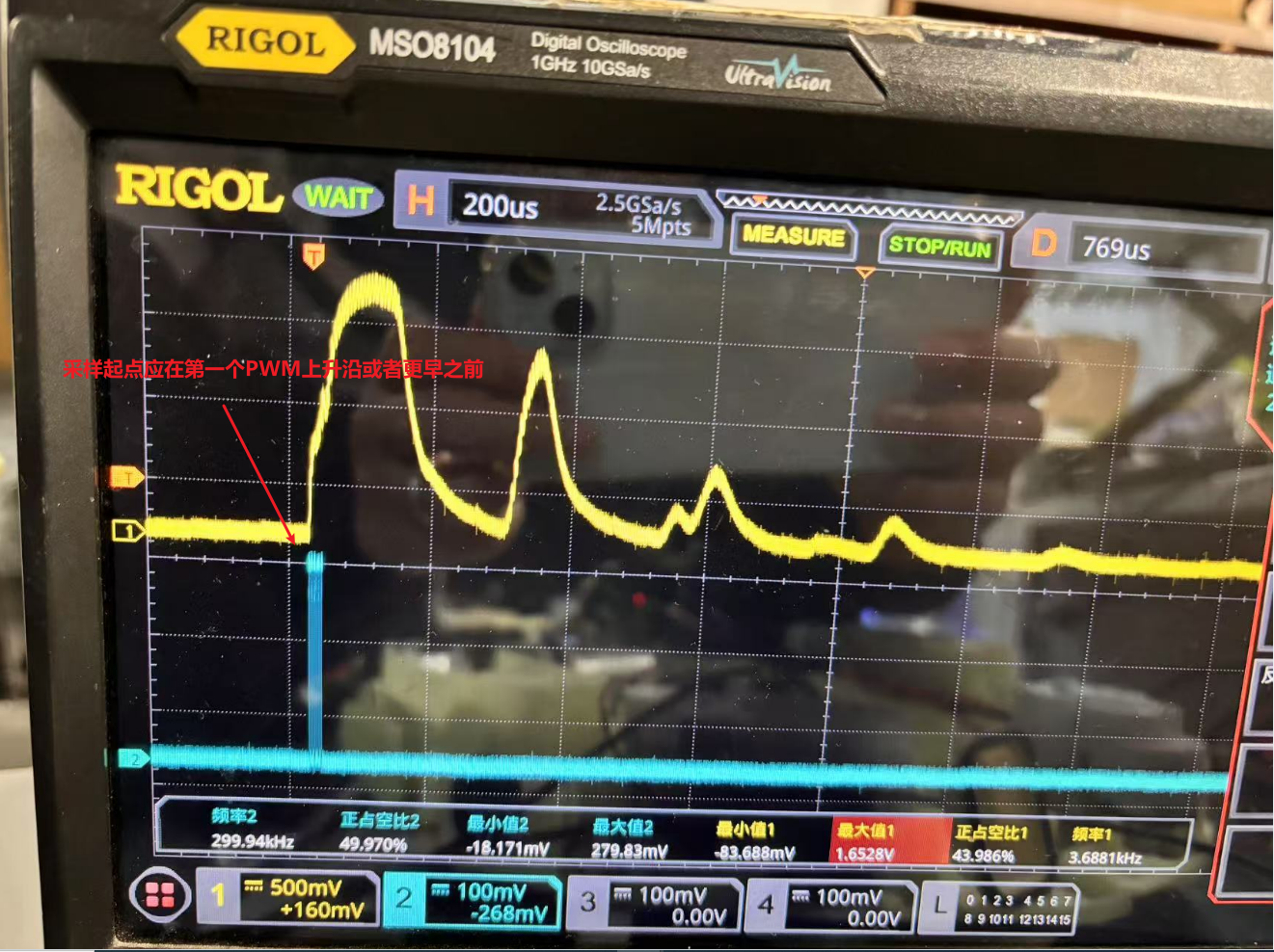
the application scenario is that the voltage (yellow) changes only after the PWM waveform (blue) is output.
If there is no error, it is just that the sampling data does not meet expectations. You need to check whether the DMA sampling timing matches the voltage change timing.
If adcmp0 is used at this time, the trigger mode of pwm_out (0~11) can be selected, and the sampling start point is the rising edge of the first PWM waveform, which can ensure that all ADC data are sampled synchronously.
If adcmp1 is used at this time, since there is no trigger mode of pwm_out, you can choose to trigger sampling first, and then control the output PWM waveform, and control the total sampling time according to the sampling count, and you can also sample all ADC data.