I2c_DebugSop
REVISION HISTORY
| Revision No. | Description |
Date |
|---|---|---|
| 1.0 | 12/13/2024 |
Issue 1: I2C Communication Failure, Unable to Capture Timing
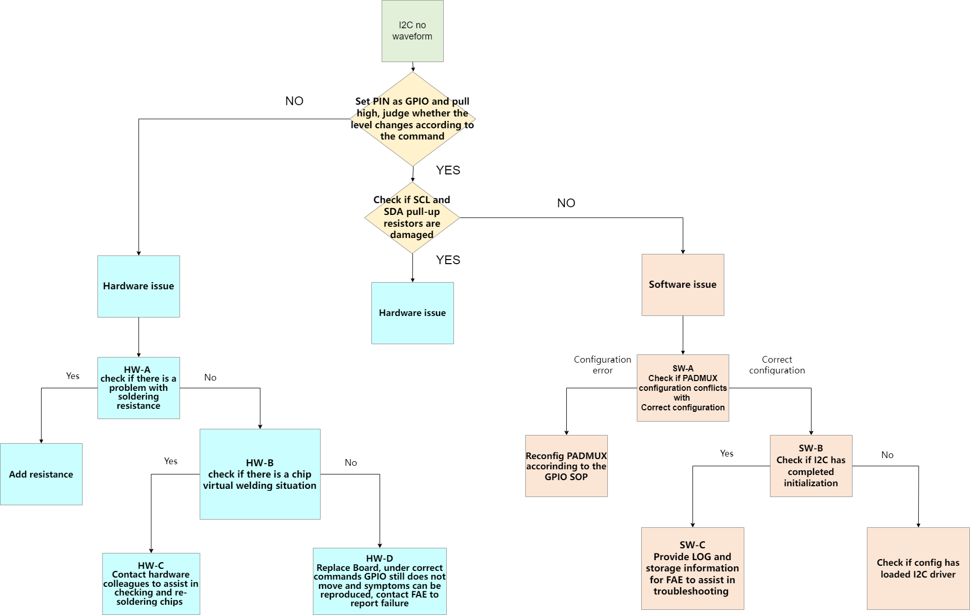
1. Debug Flowchart for I2C No Waveform Issue
2. Explanation of Debug Flow for I2C No Waveform Issue
2.1 Hardware Issues
When I2C shows no output waveform, you can manipulate the registers to set the corresponding PIN as GPIO and pull it high or low (note that some PINs may not have GPIO functionality as the highest priority, in which case you need to clear higher priority settings first). If the actual output level does not change, it can be determined to be a hardware issue, and troubleshooting can be done in the following order:
2.1.1 HW-A Check Resistors
Check if there are any soldering issues with the resistors on the corresponding PIN in the schematic. If there is a soldering issue, re-solder the resistor; otherwise, the PIN will not be functional.
2.1.2 HW-B Check Soldering Conditions
If the GPIO can be pulled high or low after changing the Board, it may indicate a cold solder joint on the chip, requiring rework.
2.1.3 HW-C Request Assistance
Contact hardware colleagues for assistance in troubleshooting and re-soldering the chip.
2.1.4 HW-D Defect Reporting
If the GPIO still cannot be pulled high or low after changing the Board, contact the FAE to report the defect.
2.2 Determine if the Pull-Up Resistors for SCL and SDA are Poorly Soldered
If the SCL and SDA pins can be switched to GPIO and can be pulled high or low normally, but when switched back to I2C MODE the IDLE level is low, it is necessary to check if the pull-up resistors are poorly soldered.
2.3 Software Issues
2.3.1 Step SW-A Check PADMUX
Check if there are any conflicts in PADMUX, refer to the PADMUX conflict check content in Gpio_DebugSop.
2.3.2 Step SW-B Check I2C Initialization Status
Dump the I2C bank; you can determine if the I2C has been initialized by checking the register status, mainly looking at whether the value at offset 0x00 is not 0x1.
When i2c0 is uninitialized, the Bank information is as follows [the following bank information takes I2C0 as an example]:

After i2c0 has been initialized, the Bank information is as follows:

| BUS | BANK | PADMUX BANK | Offset |
|---|---|---|---|
| MIIC0 | 0x1114 | 0x103c | 0x6f #[2:0] |
| MIIC1 | 0x1115 | 0x103c | 0x53 #[2:0] |
| MIIC2 | 0x1116 | 0x103c | 0x3f #[13:12] |
| MIIC3 | 0x1117 | 0x103c | 0x73 #[2:0] |
| MIIC4 | 0x1118 | 0x103c | 0x3f #[13:12] |
| PM_MIIC | 0x3E | 0x0E | 0x50 #0 |
Other I2C bank information can be found in the table above.
If initialization is not completed, it will naturally be unable to output I2C waveforms. Please check if the config and DTS configuration have loaded the I2C driver.
Linux config:
Device Drivers --->
    I2C support --->
        <*> I2C device interface
    SStar SoC platform drivers --->
        <*> Sstar I2C driver
Linux DTS:
i2c0: i2c@1f222800 {   // Select bus
    compatible = "sstar,i2c";
    reg = <0x1F222800 0x200>;
    ......
    status = "ok";    // ok: Initialize I2C
};
2.2.4 Step SW-C Request Assistance
If the above steps SW-A and SW-B are all checked and OK, please provide the I2C related error LOG and I2C BANK information (0x103c, 0x1114 (taking i2c0 as an example), 0x1038), and contact the FAE for debugging assistance.
Issue 2: NACK Phenomenon in Communication with Slave Device
1. Debug Flowchart for I2C Communication NACK Issue
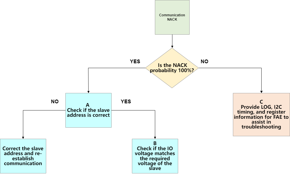
2. Explanation of Debug Flow for I2C Communication NACK Issue
2.1 Step A Check Slave Address
Currently, the slave addresses used in I2C communication are unshifted addresses. The driver will automatically left shift the received slave address by one bit before triggering communication. Please ensure not to pass in the shifted address.
2.2 Step B Check Voltage
If the pull-up voltage of SCL and SDA does not match the voltage required by the slave, the voltage of SCL and SDA cannot reach the slave's requirement, and the captured timing will generally show that after sending the slave device address, a NACK signal will be received.
2.3 Step C Request Assistance
If the above steps SW-A and SW-B are all checked and OK, please provide I2C related LOG, I2C timing, and I2C BANK information, and contact the FAE for debugging.
Issue 3: Various Irregular Timing Issues in I2C
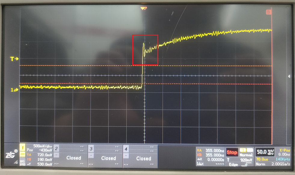
1. Overshoot Phenomenon Due to Impedance Mismatch
Impedance mismatch requires reworking the hardware; otherwise, it will directly lead to signal reflection. The reflected signal combined with the original signal will produce overshoot, ringing, step, and other signal integrity issues, as shown in the figure below:
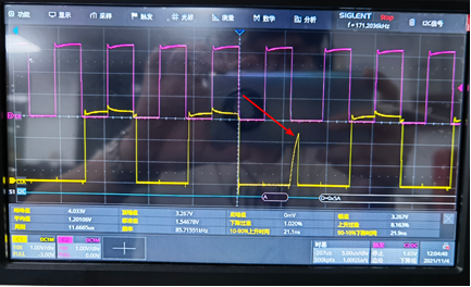
2. Short Pulses on SCL Not Complying with Standard Timing
Issues related to I2C timing at the rising edge are often related to the settings of I2C push-pull and open-drain outputs, typically manifesting as slow push high, steep slopes on the SCL rising edge, or capturing short pulses that do not comply with the timing.
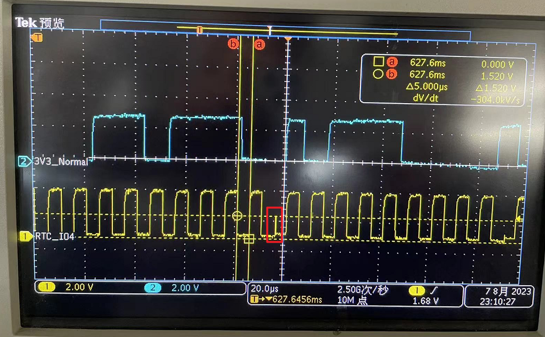
The phenomenon in the figure above is caused by the SCL using the one push function. The half high level is caused by one push; normally, it would continue to push high, but some hardware may have strong external interference, and after one push, it cannot continue to push high, resulting in a drop that causes a short pulse. You can directly disable the one push function by manipulating the registers, for example, for I2C bus0:
I2C0 Bank = 0x1114, offset = 0x00, bit[6] = 0
3. Short Pulses on SDA Not Complying with Standard Timing
When the master receives the slave ACK signal and continues to output the next bit, the PAD needs to switch from input mode to output mode. During this period, the internal pull-up resistor of the PAD generates a short pulse, which normally does not affect communication.