RISCV_I2C USER GUIDE
REVISION HISTORY
| Revision No. | Description |
Date |
|---|---|---|
| 1.0 | 04/09/2025 |
1. Overview
1.1 I2C
I2C, short for Inter-Integrated Circuit, is an integrated circuit bus that uses a multi-master to multi-slave architecture. It is a serial, synchronous, half-duplex communication bus that includes Serial Clock Line (SCL) and Serial Data Line (SDA), both of which are bidirectional IO lines. During communication, the clock signal is provided entirely by the master device; the data signal depends on whether the master device is performing a read or write operation. When performing a write operation, the data signal is provided by the master device. Conversely, when performing a read operation, the data signal is provided by the slave device.
1.2 MIIC
MIIC, or Master IIC Device, is an IP provided by SigmaStar specifically to act as the master device in I2C communications. It can communicate with various external I2C slave devices, meeting the needs of most devices that comply with the I2C communication protocol.
The relationship between device bank and hardware groups is shown in the table below:
| MIIC Group | bank addr |
|---|---|
| HW MIIC group0 | 1114H |
| HW MIIC group1 | 1115H |
| HW MIIC group2 | 1116H |
| HW MIIC group3 | 1117H |
| HW MIIC group4 | 1118H |
| HW MIIC group5 | 3EH |
2. Key Words
sysdesc:
RTOS is used to describe the hardware attributes of peripherals. The attribute values contained in the peripheral node can be used to configure the peripherals, similar to the device tree file of Linux.
padmux:
Pin Multiplexing, used to connect the functional pins of a module to specific external pins, thereby establishing signal connections.
open-drain:
Open Drain Output, does not output voltage. When controlling the pin to output a low level, the pin is grounded; when controlling the pin to output a high level, it is in a high-impedance state, with the external circuit responsible for driving the high level.
push-pull:
Push-Pull Output, capable of outputting both low and high levels. It is typically composed of two transistors or MOSFETs with similar parameters, providing strong driving capability.
3. FUNCTION DESCRIPTION
3.1 Communication Protocol
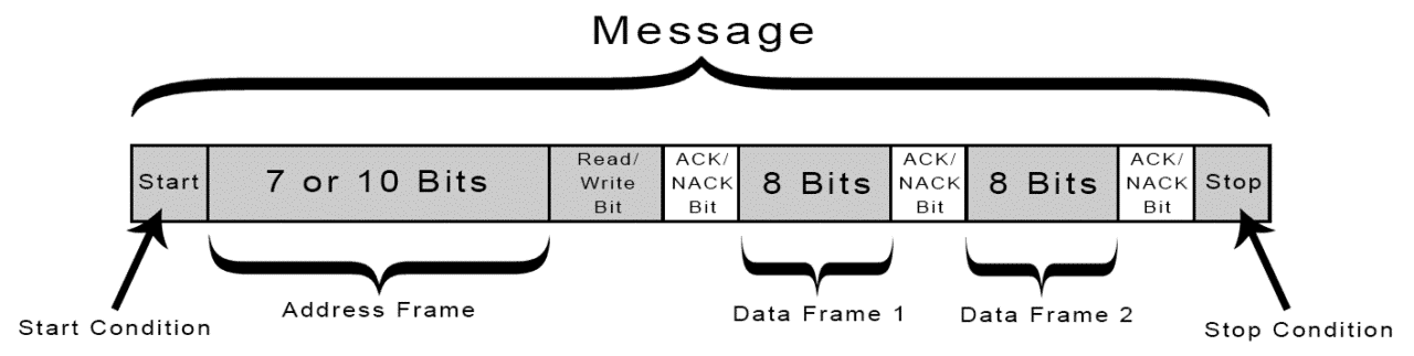
A complete I2C communication sequence must include: a Start Signal, Slave Device Address with Read/Write Bit, Acknowledge (ACK) Signal, data of arbitrary byte length, and a Stop Signal.
Start Signal: The first signal in an I2C communication sequence, generated by the master device. It indicates the beginning of communication. Electrical characteristics: SDA is pulled from high to low while SCL remains high.
Slave Device Address: Acts as the "unique identifier" for the slave device, sharing the address frame with the read/write bit. Occupies the upper 7 bits (for 7-bit addressing) or upper 10 bits (for 10-bit addressing). A slave device checks this address to determine if it is being addressed. Multiple devices with identical addresses on the same bus may cause communication failures or data corruption.
Read/Write Bit: Indicates whether the master is writing to or reading from the slave. Bit 0 (LSB) represents the operation:
0: Write operation;
1: Read operation
Example: For a 7-bit slave address 0x50 with a read operation:
address frame = (0x50 << 1) | 0x01 = 0xA1
Acknowledge (ACK) Signal: A feedback signal from the receiver (slave or master) to the sender. Low level (ACK) indicates successful reception; high level (NACK) indicates failure. During master-read operations, the master becomes the receiver after transmitting the slave address. Note: The clock (SCL) is always controlled by the master.
Data: Transmitted in byte units during read/write operations. For write operations, the slave address is typically followed by register addresses (8-bit or 16-bit), which are also treated as part of the data stream.
Stop Signal: The final signal in a communication sequence, generated by the master. It marks the end of communication. Electrical characteristics: SDA is pulled from low to high while SCL remains high.
I2C Communication Protocol Format as follow:
3.2 Function Configuration
Function |
Description |
Remark |
|---|---|---|
| FIFO transfer | Each transmission signal needs to be participated by the CPU, and different signals are sent by writing different MIIC registers | When using polling mode, the CPU loading will be relatively large; the maximum amount of data transmitted at a time is 8192 bytes; this mode is recommended when the amount of data transmitted each time is relatively small |
| DMA transfer | The entire communication process is operated by MIIC itself, and you only need to fill in the transmission content in advance and then trigger it; HW MIIC will communicate according to the timing settings that have been filled in | When using interrupt mode, the CPU loading will be smaller than FIFO mode; the maximum amount of data transmitted at a time is 4086 bytes; this mode is recommended when the amount of data transmitted each time is relatively large; when an error occurs during transmission, HW will immediately stop the communication and trigger an interrupt |
| Timing adjustment | Several I2C communication timings are available for adjustment. When a specific part of the timing does not meet the requirements of the slave device, adjust it in the dtsi node | Adjustable timing: t-SU-STA, t-HD-STA, t-SU-STO, t-HD-STO, t-SU-DAT, t-HD-DAT |
| Rate | Supports adjustable communication rate range, no gear classification, and can be adjusted in the dtsi node according to actual needs | Supports 50kHz - 1500KHz, and the higher rate requirement is not guaranteed |
| Output mode adjustment | Supports open-drain and push-pull output modes, which can be adjusted in the dtsi node | MIIC does not support arbitrary adjustment of the rising/falling edge time of the waveform, which can only be changed by adjusting the output mode, and the time cannot be confirmed. The push-pull rising edge time will be faster |
| Padmux | Different padmux can be configured to lead the bus to different pins | |
| 1toN | Some padmux will connect several groups of PAD pins at the same time, and the signal will be provided to these groups of PADs at the same time during communication | This method has the following limitations: All slave devices must be of the same type and address, and MIIC can only write data but not read data. It is generally used to connect to several identical slave devices at the same time and need to be set synchronously. |
| External pull-up | External pull-up must be connected to the I2C bus |
I2C Communication Timing as follow:
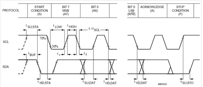
MIIC supports the following configurable timing parameters:
| Timing | Description |
|---|---|
| t-SU-STA | Start signal setup time |
| t-HD-STA | Start signal hold time |
| t-SU-STO | Stop signal setup time |
| t-HD-STO | Stop signal hold time |
| t-LOW | Clock low period |
| t-HIGH | Clock high period |
| t-SU-DAT | Data signal setup time |
| t-HD-DAT | Data signal hold time |
I2C divides communication speeds into multiple modes based on intervals:
| Speed Mode | Description |
|---|---|
| Standard-mode (Sm) | Up to 100k bit/s maximum |
| Fast-mode (Fm) | Up to 400k bit/s maximum |
| Fast-mode Plus (Fm+) | Up to 1M bit/s maximum |
| High-speed mode (Hs-mode) | Up to 3.4M bit/s maximum |
| Ultra Fast-mode (UFm) | Up to 5M bit/s maximum |
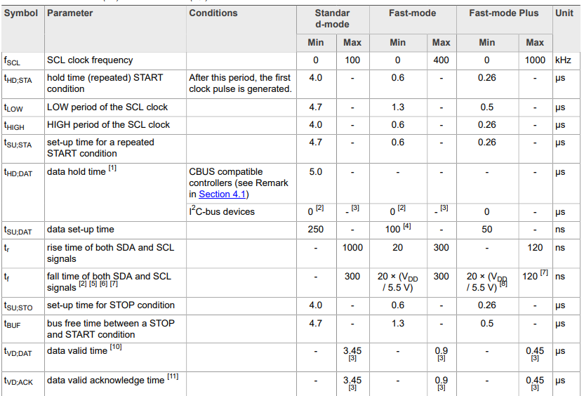
Timing Requirements for Sm/Fm/Fm+ Speed Modes as follow:
4. Introduction to Hardware Connections
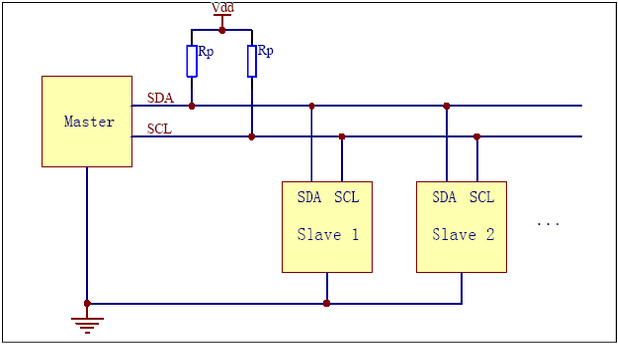
I2C follows a multi-master, multi-slave architecture. By definition, a single bus can host multiple master devices and multiple slave devices. Communication between devices is established through slave addresses and acknowledge (ACK) signals.
SigmaStar's I2C only provides one MIIC (master iic) master device on each bus, and there is no requirement for the number of slave devices, which can be set according to usage requirements.
In addition, in accordance with the I2C standard protocol, the external pull-up must be connected to the SDA and SCL of the bus. This is because I2C communication requires the ability to output a high level, and when the device output is an open-drain output, it cannot output a high level. At this time, the help of an external pull-up is needed to realize the "Wired-AND" function and determine the final level.
The following is an example diagram of the I2C bus:
5. RTOS USAGE INTRODUCTION
5.1. DRIVER PATH
sc/driver/sysdriver/i2c/os/iic_os.h
sc/driver/sysdriver/i2c/drv/pub/drv_iic.h
sc/driver/sysdriver/i2c/drv/src/drv_iic.c
sc/driver/sysdriver/i2c/drv/src/drv_iic_test.c
sc/driver/sysdriver/i2c/hal/pcupid/src/hal_iic.c
sc/driver/sysdriver/i2c/hal/pcupid/inc/hal_iic.h
sc/driver/sysdriver/i2c/hal/pcupid/inc/hal_iic_reg.h
sc/driver/sysdriver/i2c/hal/pcupid/inc/hal_iic_cfg.h
5.2. CONFIG Configuration
config locate in mak/options_chipname_riscv_isw.mak,and enable CONFIG_I2C_SUPPORT
# Feature_Name = [DRV] I2C driver support
# Description = I2C driver support
# Option_Selection = TRUE, FALSE
# CONFIG_I2C_SUPPORT = TRUE
5.3. SYSDESC Configuration
pcupid-default.sys file is located in sc\driver\sysdriver\sysdesc\hal\pcupid\pub\.
<i2c0>
    [reg_u32_u16] 0x2222800 0x200;
    [interrupts_u8] INT_IRQ_MIIC;
    [camclk_u16] CAMCLK_miic0;
    [dma_u8] 1;
    [output_mode_u8] 2;
    [speed_u32] 200000;
    [t_su_sta_u32] 0;
    [t_hd_sta_u32] 0;
    [t_su_sto_u32] 0;
    [t_hd_sto_u32] 0;
    [t_su_dat_u32] 0;
    [t_hd_dat_u32] 0;
    [status_u8] 1;
The attributes supported for configuration in the Master IIC driver are as follows:
| Attribute | Description | Setting value | Remark |
|---|---|---|---|
| reg_u32_u16 | Specify the address of the bank | No modification required | |
| interrupts_u8 | Specify the hardware interrupt number | No modification required | |
| dma_u8 | Select whether to enable DMA mode | 1-enable; 0-disable | Can be modified as needed |
| output_mode_u8 | Select the output mode | 1: open drain output; 2: open drain push 1T output; 3: open drain push 1T strong pull-up; 4: push-pull output | Can be modified as needed,1->4 rising edge time is shortened in turn |
| speed_u32 | Set the communication frequency, the unit is HZ | Range 50K~1500K HZ | Can be modified as needed |
| t_su_sta_u32 | Set the start signal hold time | ns value | Can be modified as needed |
| t_hd_sta_u32 | Set the start signal establishment time | ns value | Can be modified as needed |
| t_su_sto_u32 | Set the end signal establishment time | ns value | Can be modified as needed |
| t_hd_sto_u32 | Set the end signal hold time | ns value | Can be modified as needed |
| t_su_dat_u32 | Set the end signal establishment time | ns value | Can be modified as needed |
| t_hd_dat_u32 | Set the start signal establishment time | ns value | Can be modified as needed |
| camclk_u16 | Specify the clock source | No modification required | |
| status_u8 | Select whether to enable the driver | 1-enable; 0-disable | Can be modified as needed |
Detailed description:
Figure 5-1 below shows the detailed timing decomposition of miic, and Figure 5-2 shows the positions of several adjustable timings.
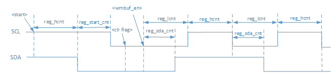
Figure 5-1: MIIC Communication Timing
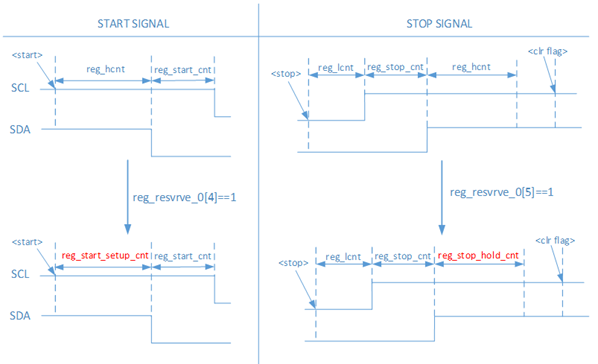
Figure 5-2: MIIC Start Signal and End Signal Timing Adjustment
Several timing adjustments are available in sysdesc, and the corresponding waveform positions are:
Timing |
Waveform Position |
|---|---|
| t-su-sta | reg_start_setup_cnt |
| t-hd-sta | reg_start_cnt |
| t-su-sto | reg_stop_cnt |
| t-hd-sto | reg_stop_hold_cnt |
| t-su-dat | reg_lcnt - reg_sda_cnt |
| t-hd-dat | reg_sda_cnt |
If the attribute value in the node is 0, the driver will calculate the ns value according to the established calculation. If there is a setting, it will follow the setting value. The theoretical maximum value of the setting is U32_MAX, unit is ns.
5.4. PADMUX Configuration
CONFIG Configuration: CONFIG_PADMUX_SUPPORT=TRUE
If the chipname_xxx.sys file is configured with the attribute <padmux>, then the PADMUX setting is directly configured here:
<padmux>
    [schematic_u32_u32_u32]
        PAD_GPIOE_01    PINMUX_FOR_I2C0_MODE_1    MDRV_PUSE_I2C0_SDA,
        PAD_GPIOE_04    PINMUX_FOR_I2C1_MODE_1    MDRV_PUSE_I2C1_SCL,
        PAD_GPIOE_05    PINMUX_FOR_I2C1_MODE_1    MDRV_PUSE_I2C1_SDA,
        PAD_GPIOE_21    PINMUX_FOR_I2C2_MODE_1    MDRV_PUSE_I2C2_SCL,
        PAD_GPIOE_22    PINMUX_FOR_I2C2_MODE_1    MDRV_PUSE_I2C2_SDA,
        PAD_GPIOE_23    PINMUX_FOR_I2C3_MODE_1    MDRV_PUSE_I2C3_SCL,
        PAD_GPIOE_24    PINMUX_FOR_I2C3_MODE_1    MDRV_PUSE_I2C3_SDA,
        PAD_GPIOD_01    PINMUX_FOR_I2C4_MODE_1    MDRV_PUSE_I2C4_SCL,
        PAD_GPIOD_02    PINMUX_FOR_I2C4_MODE_1    MDRV_PUSE_I2C4_SDA,
        PAD_PM_I2C_SDA    PINMUX_FOR_PM_I2CM0_MODE_1    MDRV_PUSE_I2C5_SCL,
        PAD_PM_I2C_SDA    PINMUX_FOR_PM_I2CM0_MODE_1    MDRV_PUSE_I2C5_SDA,
    [status_u8] 1;
Otherwise, enable the PADMUX driver and configure the pin multiplexing function in the chipname-xxx-padmux.c file, which is located in sc/driver/sysdriver/padmux/hal/chipname/src. You only need to add the following content to the corresponding schematic attribute:
pad_info_t schematic[] =
{
    {PAD_GPIOE_01    PINMUX_FOR_I2C0_MODE_1    MDRV_PUSE_I2C0_SDA},
    {PAD_GPIOE_04    PINMUX_FOR_I2C1_MODE_1    MDRV_PUSE_I2C1_SCL},
    {PAD_GPIOE_05    PINMUX_FOR_I2C1_MODE_1    MDRV_PUSE_I2C1_SDA},
    {PAD_GPIOE_21    PINMUX_FOR_I2C2_MODE_1    MDRV_PUSE_I2C2_SCL},
    {PAD_GPIOE_22    PINMUX_FOR_I2C2_MODE_1    MDRV_PUSE_I2C2_SDA},
    {PAD_GPIOE_23    PINMUX_FOR_I2C3_MODE_1    MDRV_PUSE_I2C3_SCL},
    {PAD_GPIOE_24    PINMUX_FOR_I2C3_MODE_1    MDRV_PUSE_I2C3_SDA},
    {PAD_GPIOD_01    PINMUX_FOR_I2C4_MODE_1    MDRV_PUSE_I2C4_SCL},
    {PAD_GPIOD_02    PINMUX_FOR_I2C4_MODE_1    MDRV_PUSE_I2C4_SDA},
    {PAD_PM_I2C_SDA    PINMUX_FOR_PM_I2CM0_MODE_1    MDRV_PUSE_I2C5_SCL},
    {PAD_PM_I2C_SDA    PINMUX_FOR_PM_I2CM0_MODE_1    MDRV_PUSE_I2C5_SDA},
};
The first column is the pin index number, which can be queried in sc/drivers/sysdriver/gpio/hal/chipname/pub/gpio.h;
The second column is the mode definition, which can be queried in sc/drivers/sysdriver/gpio/hal/chipname/pub/padmux.h;
The third column is the index name of the pin and matching mode, which can be queried in sc/drivers/sysdriver/padmux/drv/pub/drv_puse.h.
5.5 Sample code
The header file is located in sc/driver/sysdriver/i2c/drv/pub/drv_iic.h.
static int i2c_ut_test(CLI_t * cli, char * p)
{
    u8 i;
    u8 argc;
    u32 port;
    u32 slave;
    char *cmd;
    tI2cMsg msg;
    u32 addr;
    u32 value;
    u8 data[32];
    u8 e_data[32];
    int ret   = 0;
    u8 r_flag = 0;
    u32 speed = 0;

    argc = CliTokenCount(cli);
    if (argc < 2)
        return eCLI_PARSE_INPUT_ERROR;

    cmd = CliTokenPop(cli);
    if (strcmp(cmd, "r") == 0)
    {
        argc = CliTokenCount(cli);
        if (argc != 4)
            return eCLI_PARSE_INPUT_ERROR;
        r_flag = 1;

    }
    else if (strcmp(cmd, "w") == 0)
    {
        argc = CliTokenCount(cli);
        if (argc < 5 || argc > 6)
            return eCLI_PARSE_INPUT_ERROR;
    }
    else
    {
        return eCLI_PARSE_INPUT_ERROR;
    }

    if (CliTokenPopNum(cli, &port, 0) != eCLI_PARSE_OK)
    {
        return eCLI_PARSE_INPUT_ERROR;
    }

    if (CliTokenPopNum(cli, &slave, 0) != eCLI_PARSE_OK)
    {
        return eCLI_PARSE_INPUT_ERROR;
    }

    cmd = CliTokenPop(cli);
    if (strcmp(cmd, "A16D8") == 0)
    {
        msg.addr = (u16)slave;
        if (r_flag)
        {
            if (CliTokenPopNum(cli, &addr, 0) != eCLI_PARSE_OK)
            {
                return eCLI_PARSE_INPUT_ERROR;
            }

            //write
            msg.flags = 0;
            data[0] = (u8)((addr >> 8) & 0xff);
            data[1] = (u8)(addr & 0xff);
            msg.buf = data;
            msg.len = 2;
            drv_i2c_master_xfer(port, &msg, 1);

            //read
            msg.flags = CAM_I2C_RD;
            msg.buf = data;
            msg.len = 1;
            drv_i2c_master_xfer(port, &msg, 1);
            cliPrintf(" %04x : %02x\r\n", (u16)addr, (u8)data[0]);
        }
        else
        {
            if (CliTokenPopNum(cli, &addr, 0) != eCLI_PARSE_OK)
            {
                return eCLI_PARSE_INPUT_ERROR;
            }

            if (CliTokenPopNum(cli, &value, 0) != eCLI_PARSE_OK)
            {
                return eCLI_PARSE_INPUT_ERROR;
            }

            CliTokenPopNum(cli, &speed, 0);

            data[0] = (u8)((addr >> 8) & 0xff);
            data[1] = (u8)(addr & 0xff);
            data[2] = (u8)(value & 0xff);

            //write
            msg.flags = 0;
            msg.buf = data;
            msg.len = 3;

            //set i2c speed
            if (speed)
                drv_i2c_set_speed(port, speed);

            //transfer
            drv_i2c_master_xfer(port, &msg, 1);
        }

    }

    return eCLI_PARSE_OK;
}
6. API Reference
This functional module provides the following interfaces:
| API | Function |
|---|---|
| drv_i2c_master_xfer | Perform IIC transfer (synchronous) |
| drv_i2c_set_speed | Set iic tranfer speed |
To use these APIs, you need to include the header file sc/driver/sysdriver/i2c/drv/pub/drv_iic.h.
The data structures defined within it are as follows:
typedef struct i2c_msg {
    u16 addr;   /*slave address*/
    u16 flags;
#define CAM_I2C_RD                   0x0001
#define CAM_I2C_STOP_BEFORE_RESTART  0x0002
#define CAM_I2C_TEN                  0x0010
#define CAM_I2C_DMA_SAFE             0x0200
#define CAM_I2C_RECV_LEN             0x0400
#define CAM_I2C_NO_RD_ACK            0x0800
#define CAM_I2C_IGNORE_NAK           0x1000
#define CAM_I2C_REV_DIR_ADDR         0x2000
#define CAM_I2C_NOSTART              0x4000
#define CAM_I2C_STOP                 0x8000
    u16 len;        /*msg length*/
    u8 *buf;        /*pointer to msg data*/
}tI2cMsg;
6.1. drv_i2c_master_xfer
-
Function
Perform a single synchronous IIC transfer with the IIC channel corresponding to para_group, using para_num para_msg entries to store the transfer information.
-
Declaration
s32 drv_i2c_master_xfer(u8 para_group, struct i2c_msg *para_msg, s32 para_num);
-
Parameters
Parameter Name Description para_group Device Number para_msg Communication Content para_num Information Length -
Return Value
Return Value Description 0 Failure positive Success
6.2 drv_i2c_set_speed
-
Function
Set speed of the IIC channel corresponding to para_group to speed
-
Declaration
s32 drv_i2c_set_speed(u8 para_group, u32 speed);
-
Parameters
Parameter Name Description para_group i2c bus speed Transfer frequence, units is Hz -
Return Value
Return Value Description 0 Success other Failure
7. DEBUG
When communication abnormalities occur, you can refer to the following aspects for troubleshooting. Several common troubleshooting directions are provided. Additionally, it is recommended to capture waveforms during the debugging process for easier analysis.
| Troubleshooting Directions | Common Issues |
Note |
|---|---|---|
| External Pull-up | 1. Indicates a communication timeout error message; 2. Captured waveform shows no change, SCL remains low; 3. The data read and written in the captured waveform are all 0x00; | |
| padmux | 1. Indicates no ACK signal;2. The waveform shows no change, the level remains constant; | Refer to the PADMUX chapter, or the padmux module description; |
| Communication Rate | Communication failed, no ACK signal; | Check the slave device manual to confirm the normal operating communication rate range; |
| Clock Source | 1. Indicates a communication timeout error message;2. No waveform; | Refer to the CLKGEN module description; |
| Timing | Communication has no ACK signal; | If the slave device has specific requirements for detailed timing, check and confirm these from the device manual; |
| Slave Device Operating State | Communication has no ACK signal; | When the slave device is not in a normal working state, it cannot respond to signals initiated by the master device; |