Comake PI D1 Hardware Description
REVISION HISTORY
| Revision No. | Description |
Date |
|---|---|---|
| 1.0 | 07/26/2025 | |
1. Introduction to Comake PI D1 V1.0
This guide will help you quickly get started with the COMAKE PI D1 development board and provide detailed information about this development board. The COMAKE PI D1 development board is based on the SSD2355 chip.
1.1. System Overview
- The main chip SSD2355 uses a quad-core ARM Cortex-A35 with a maximum frequency of 1.5GHz;
- Onboard external 16bit 8Gbit DDR4-3200MHz;
- Onboard Flash: SPI Nand Flash 1G bit / SPI Nor Flash 128M bit;
- Supports 5-inch MIPI Panel (maximum interface 2560*1600@60fps);
- Supports 2lane or 1lane + 1lane MIPI RX interface;
- Supports WIFI6/BLE5.2/dual-band 2.4G&5G;
- Supports 2 USB2.0 ports (can be configured as host or device via software), with USB P1 default connected to SSW108GE USB WIFI Module;
- Supports dual Ethernet ports 100/10M auto-adaptive;
- Supports 24-channel 12-bit precision ADC and 5-channel 10-bit precision ADC;
- Supports 3-channel AMIC differential input;
- Supports 8 CH DMIC input;
- Supports Lineout single-ended dual-channel output;
- Reserved 40-pin GPIO, which can be configured for other functions, such as TTL screen, FUART, etc.;
- VDD_CPU voltage: default 1V, software configurable to adjust voltage according to frequency;
- VDD_Core voltage: default 1V;
- DRAM voltage: DDR4-1.2V/2.5V;
- IO voltage: 1.8V/3.3V;
- Chip normal operating temperature range: -20°C ~ +70°C;
- Power input: 12V 1A, or 5V 2A (Micro USB);
- Supports POC (current setting requires pressing the S5 POWER KEY to power on).
2. Interface Module Diagram
2.1. Interface Module Schematic
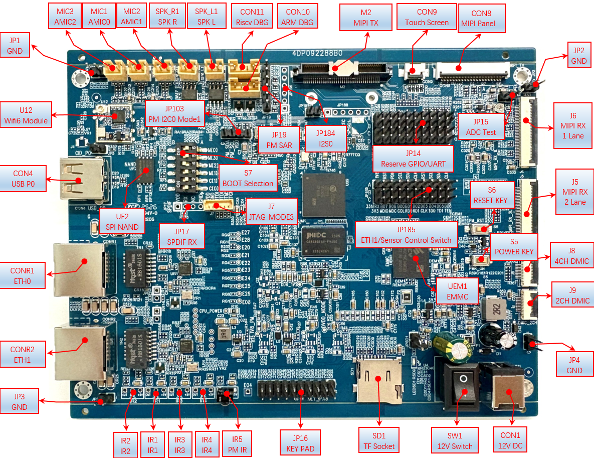
| Major Components | Description (see later sections for details) |
|---|---|
| DC 12V 1A(CON1) | CON1 is the DC 12V power interface |
| DC 12V Power Switch (SW1) | SW1 is the DC 12V power switch. |
| POWER KEY (S5) | Pressing the POWER KEY will power on the SOC and the indicator light will turn on. |
| RESET KEY(S6) | Pressing the RESET KEY will reboot the SOC. |
| Arm Debug Uart Interface (CON10) | Arm Debug Uart, default baud rate is 115200 |
| RISC-V Debug Uart Interface (CON11) | RISC-V Debug Uart, default baud rate is 115200 |
| Left Channel Speaker Interface (SPK_L) | SPK_L is reserved for AEC circuit returned to MIC0, used for hardware AEC. |
| Right Channel Speaker Interface (SPK_R) | SPK_R is reserved for AEC circuit returned to MIC1 for hardware AEC. |
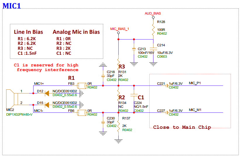
| Analog Microphone ch1 and Line In Interface (MIC1) | MIC1 is default connected to the microphone. To connect Line In, the voltage divider on the board needs to be modified. |
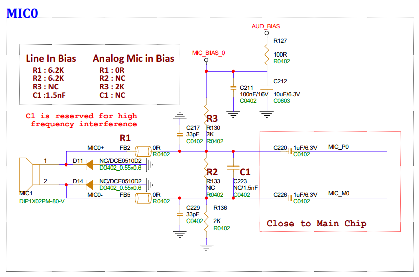
| Analog Microphone ch0 and Line In Interface (MIC0) | MIC0 is default connected to the microphone. To connect Line In, the voltage divider on the board needs to be modified, same as MIC1. |
| Analog Microphone ch2 and Line In Interface (MIC2) | MIC2 is default connected to the microphone. To connect Line In, the voltage divider on the board needs to be modified, same as MIC1. |
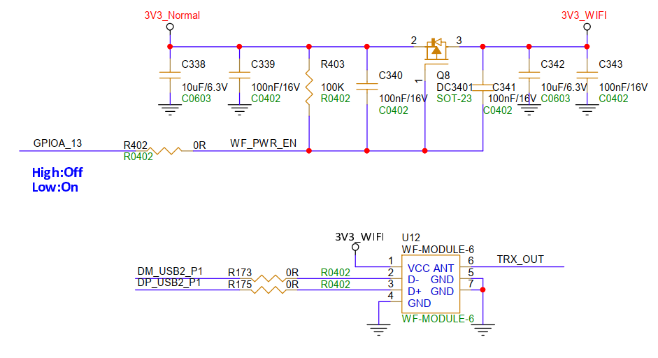
| SSW108GE USB WIFI Module (U12) | USB P1 is default configured as USB Host, connected with SSW108GE USB WIFI Module, and supports configuration to Device mode if needed. The power supply for the SSW108GE module needs to be controlled via GPIOA13, pull low to turn on WIFI power. |
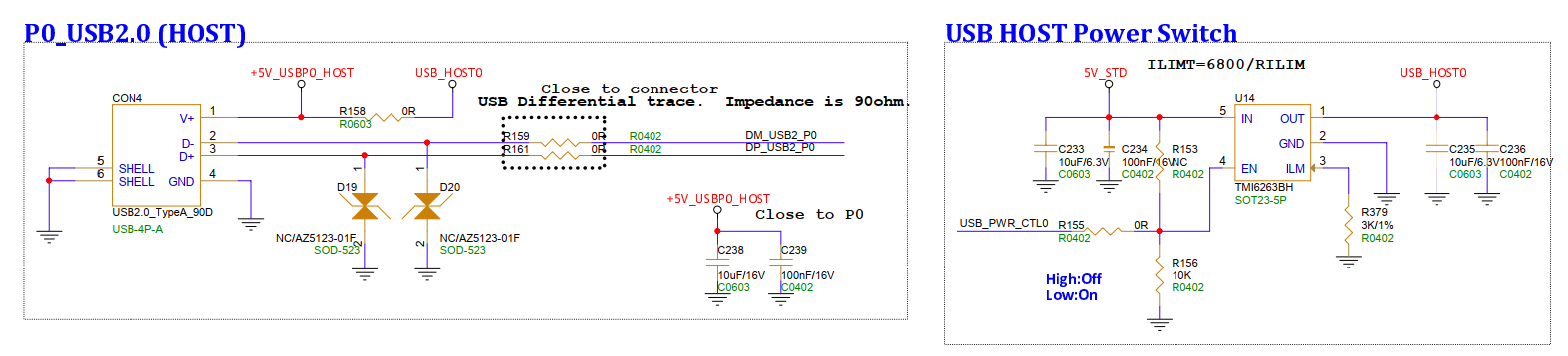
| USB 2.0 P0 Interface (CON4, CON5) | P0 can be configured as Host or Device via software. The A port (CON4) can power external devices when used as a host, requiring GPIOA_10 to be pulled high to enable the power; the microB port (CON5) can power the mainboard. |
| SPI NAND(UF2) | UF2 1Gb SPI NAND, supports SPI NAND boot, configuration switch S7 is needed for boot selection. |
| SPDIF RX(JP17) | SPDIF IN Mode4, can connect to SPDIF receiver socket for sub-board or directly connect to SPDIF signal. |
| Boot Selection Switch (S7) | A switch used for selecting boot and upgrade modes. |
| PM I2C0 Mode1(JP103) | Reserved I2C for debugging external devices. |
| JTAG (J7) | Can be configured to switch between ARM mode3 or RSICV Mode2 for debugging ARM or RSICV. |
| PM SARADC Reserved Interface (JP19) | Reserved PM_SARADC interface for detecting external analog levels. |
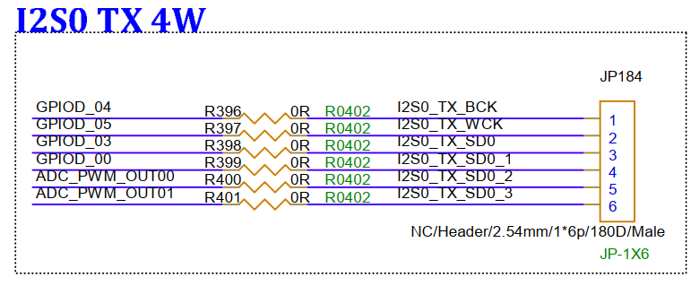
| I2S0 4W TX Interface(JP184) | I2S0 interface. |
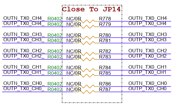
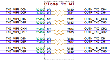
| MIPI TX Interface(M2) | MIPI TX interface, can connect to MIPI to HDMI accessories to connect displays. However, for signal quality, the MIPI screen connection to M2 will be broken by default. If using MIPI to HDMI, the following 0R resistors (R778-R787) need to be added and M2 cannot be used simultaneously with the MIPI screen. |
| MIPI Panel (5-inch 40Pin) interface (CON8) | CON8 MIPI screen and M2 connector signal will be multiplexed and cannot be used simultaneously. The MIPI screen is connected via FPC, make sure not to reverse the connection. |
| Touch Screen Interface (CON9) | The touch screen is default left-side sequence, the default is a reversed FPC flat cable. |
| GPIO Reserved (JP14) | This part of IO is reserved for pin headers and can be configured for other functions, such as TTL screens. Supported functions can be found in the HW checklist of ARM Tmux. |
| ETH and Sensor Control Selection (JP185) | Due to IO allocation, there is a conflict with ETH1 and sensor control signals. Currently, it is selected using a jumper cap. The factory default is the sensor interface, with JP185 fully connected to A-B. If ETH1 is needed, JP185 jumper caps must be connected completely to B-C. Note: To enable ETH1, the dts configuration needs to be modified. For specifics, you can refer to the DTS node enabling EMAC1 example |
| EMMC(UEM1) | EMMC supports EMMC5.0, HS200/400 by default. |
| SAR TEST(JP15) | The board has a reserved sliding rheostat for SAR testing, which can be pulled to other SAR ports for validation and voltage adjustment using VR2. |
| SR MIPI RX 1lane(J6) | J6 connects to a 1Lane MIPI Sensor. |
| SR MIPI RX 2lane(J5) | J5 is default connected to a 1lane MIPI Sensor, but can also connect to a 2lane MIPI Sensor; when connecting to a 2lane MIPI Sensor, there is a multiplexing relationship between J6 and J5 (CH2P/N) and both cannot be used together. When connecting to a 1lane MIPI sensor, J6 and J5 can be used simultaneously. |
| DMIC(J8/J9) | J8 is for 4Ch DMIC, supporting up to 8 DMICs; J9 is for 2Ch DMIC, supporting up to 4 DMICs; Note:there is a multiplexing relationship between J8 and J9, D2/D3 cannot be used simultaneously. After using D2/D3 on J9, J8 can only connect to D0/D1 for 2ch.It is recommended to use J8 by default. |
| TF Card Slot (SD1) | Note: EMMC and SD interfaces share a power domain, the default voltage for EMMC is 1.8V. At this time, the SD1 TF interface cannot use a TF card but can use 1.8V SDIO Wifi. |
| KEY PAD(JP16) | Reserved KEY PAD interface, can be connected as a matrix keyboard or to I2S; note that when connecting a matrix keyboard, it cannot be shared with IR and ETH. |
| PM_IR(IR5) | IR reception interface for RISCV. |
| IR1 2 3 4(IR1 2 3 4) | IR reception interface for ARM, not yet mounted by default. |
| ETH0(CONR1) | CONR1 is the ETH0 100Mbps ethernet interface 0. |
| ETH1(CONR2) | CONR2 is the ETH1 100Mbps ethernet interface 1. Note: By default, it is not available; JP185 jumper caps need to be entirely changed to B-C. |
3. Detailed Description of Some Interface Modules
3.1. DC 12V 1A(CON1)
CON1 is the DC 12V power interface.
3.2. DC 12V Power Switch (SW1)
SW1 is the DC 12V power switch. Note: This switch only turns on the 12V power; to truly power on the system, the POWER KEY must be pressed, and the indicator light will also turn on.
3.3. POWER KEY (S5)
Pressing the POWER KEY will power on the SOC and the indicator light will turn on.
3.4. RESET KEY(S6)
Pressing the RESET KEY will reboot the SOC.
3.5. Arm Debug Uart Interface (CON10)
Arm Debug Uart, default baud rate is 115200. CON10 can also switch to I2C mode, using SigmaStar ISP Tool to upgrade uboot and read register information.
3.6. RISC-V Debug Uart Interface (CON11)
RISC-V Debug Uart, default baud rate is 115200.
3.7. Left Channel Speaker Interface (SPK_L)
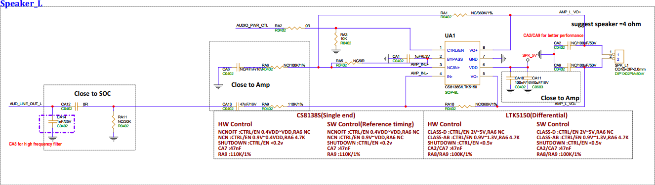
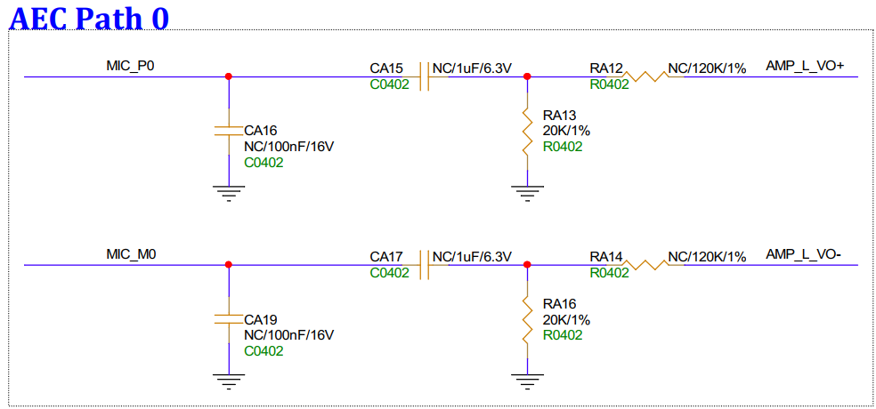 SPK_L is reserved for the AEC circuit returned to MIC0, used for hardware AEC.
3.8. Right Channel Speaker Interface (SPK_R)
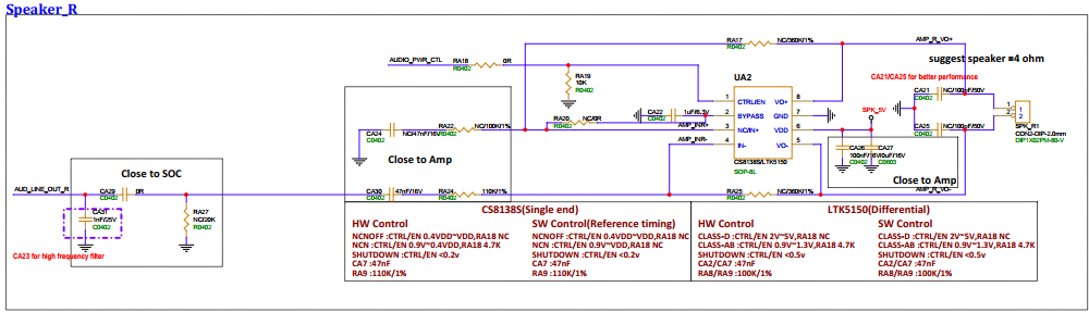
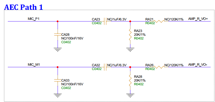 SPK_R is reserved for the AEC circuit returned to MIC1 for hardware AEC.
3.9. Analog Microphone ch1 and Line In Interface (MIC1)
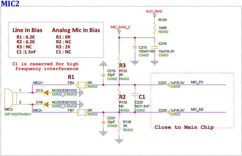
MIC1 is default connected to the microphone. To connect Line In, the voltage divider on the board needs to be modified, see the following image:
3.10. Analog Microphone ch0 and Line In Interface (MIC0)
MIC0 is default connected to the microphone. To connect Line In, the voltage divider on the board needs to be modified, same as MIC1.
3.11. Analog Microphone ch2 and Line In Interface (MIC2)
MIC2 is default connected to the microphone. To connect Line In, the voltage divider on the board needs to be modified, same as MIC1.
3.12. SSW108GE USB WIFI Module (U12)
USB P1 is default configured as USB Host, connected with SSW108GE USB WIFI Module, and supports configuration to Device mode if needed. The power supply for the SSW108GE module needs to be controlled via GPIOA13, pull low to turn on WIFI power.
3.13. USB 2.0 P0 Interface (CON4, CON5)
P0 can be configured as Host or Device via software. The A port (CON4) can power external devices when used as a host, requiring GPIOA_10 to be pulled high to enable the power; the microB port (CON5) can power the mainboard.

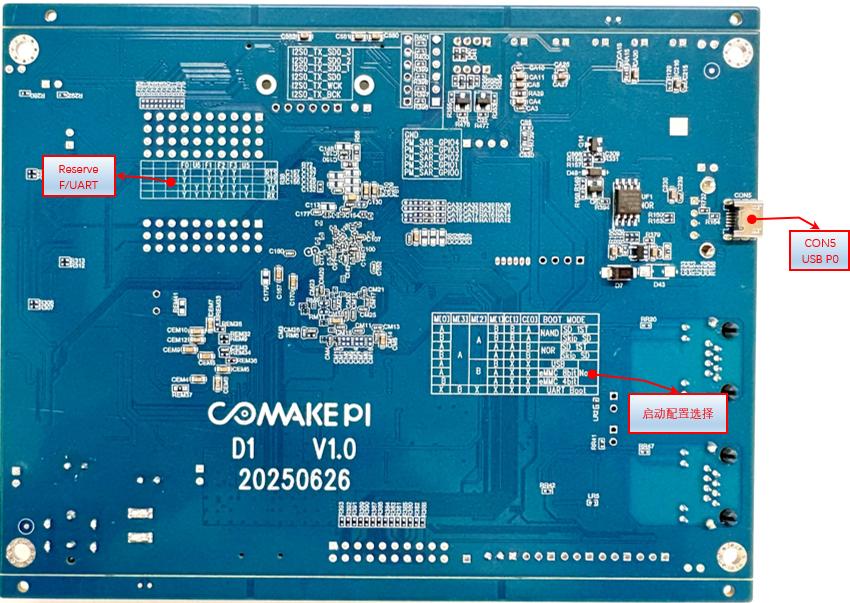
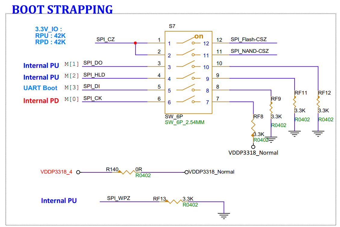
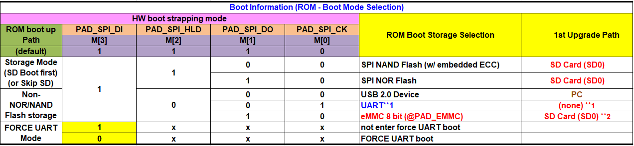
3.14. SPI NAND(UF2)
UF2 1Gb SPI NAND, supports SPI NAND boot, configuration switch S7 is needed for boot selection.
3.15. SPDIF RX(JP17)
SPDIF IN Mode4, can connect to SPDIF receiver socket for sub-board or directly connect to SPDIF signal.
3.16. Boot Selection Switch (S7)
A switch used for selecting boot and upgrade modes;
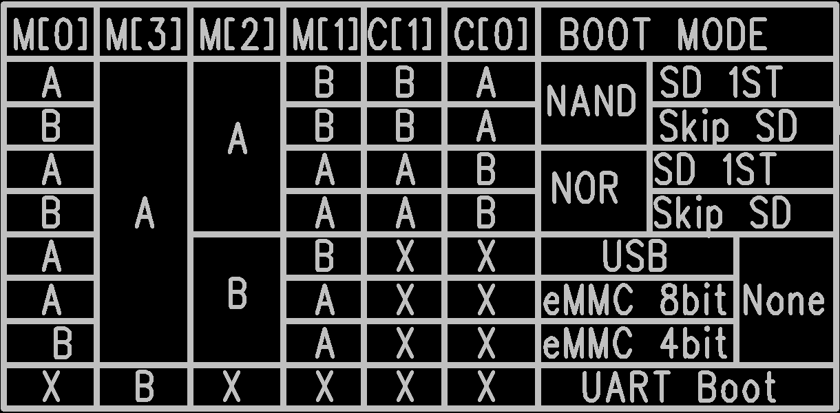
-
For example, to boot from EMMC, if you need to set EMMC to operate in 8-bit mode, then “M[0],M[3],M[2],M[1]”=“AABA”, “C[1],C[0] ” can be ignored, then power on.
If you need to set EMMC to operate in 4-bit mode, then “M[0],M[3],M[2],M[1],C[1],C[0]”=“BABA”, “C[1],C[0] ” can be ignored, then power on.
-
For example, to skip detection of the SD card (SD0 only supports card booting, the board default is SD1 which is not supported) and boot directly from SPI NAND, “M[0],M[3],M[2],M[1],C[1],C[0]”= “AAABBA”
-
For example, to skip detection of the SD card (SD0 only supports card booting, the board default is SD1 which is not supported) and boot directly from SPI NOR, “M[0],M[3],M[2],M[1],C[1],C[0]”= “BAAAAB”
3.17. PM I2C0 Mode1(JP103)
Reserved I2C for debugging external devices.
3.18. JTAG (J7)
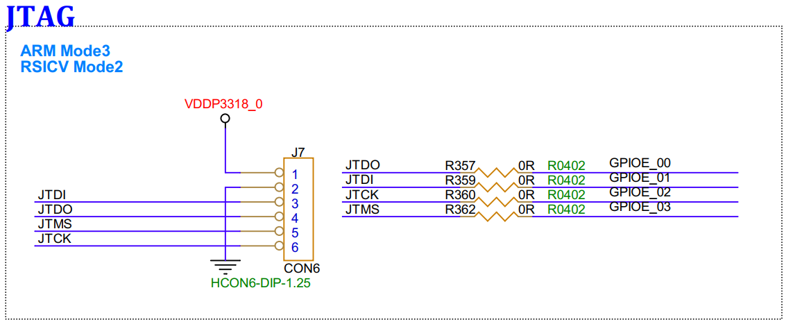
Can be configured to switch between ARM mode3 or RSICV Mode2 for debugging ARM or RSICV.
3.19. PM SARADC Reserved Interface (JP19)
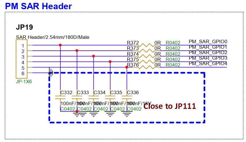
Reserved PM_SARADC interface for detecting external analog levels. PM_SAR_GPIO0 is used for peripheral 5V enable control, please pay attention when using it.
3.20. I2S0 4W TX Interface (JP184)
3.21. MIPI TX Interface (M2)
MIPI TX interface, can connect to MIPI to HDMI accessories to connect displays. However, for signal quality, the MIPI screen connection to M2 will be broken by default. If using MIPI to HDMI, the following 0R resistors (R778-R787) need to be added and M2 cannot be used simultaneously with the MIPI screen.
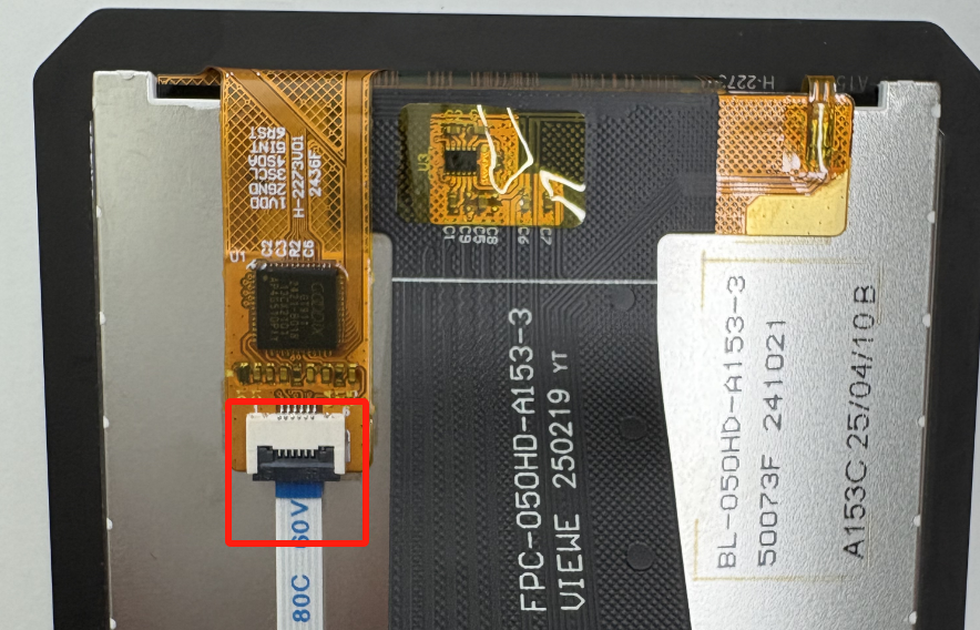
3.22. MIPI Panel (5-inch 40Pin) Interface (CON8)
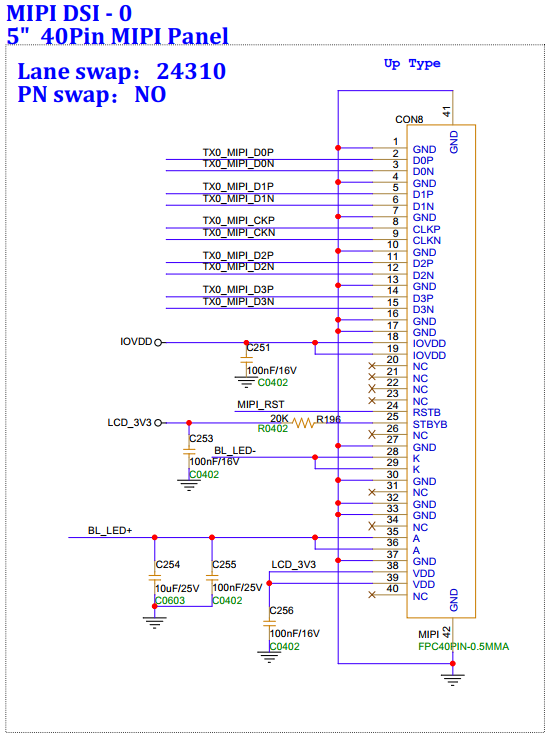
Note: CON8 MIPI screen and M2 connector signal will be multiplexed and cannot be used simultaneously. The MIPI screen is connected via FPC, make sure not to reverse the connection, see the following image.
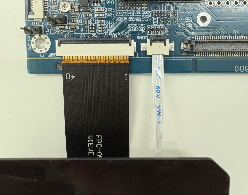
3.23. Touch Screen Interface (CON9)
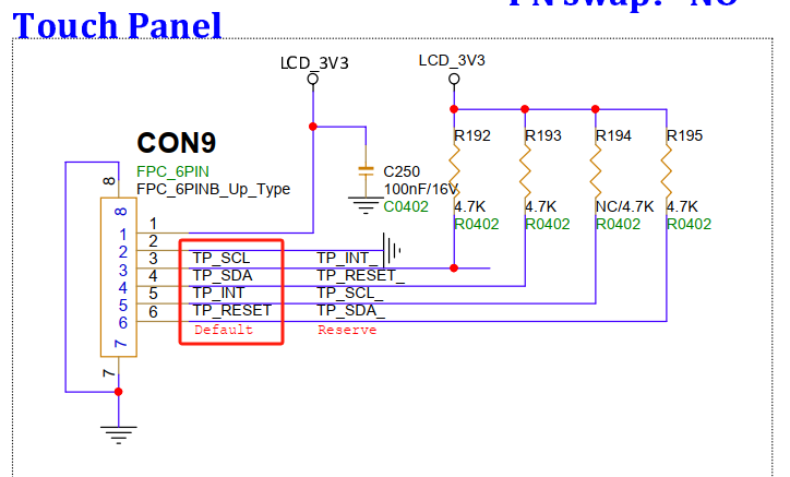
The touch screen is default left-side sequence, the default is a reversed FPC flat cable.
Note: The side close to the screen is for FPC down connection, and the side close to the mainboard is for FPC up connection, make sure not to reverse.
3.24. GPIO Reserved (JP14)
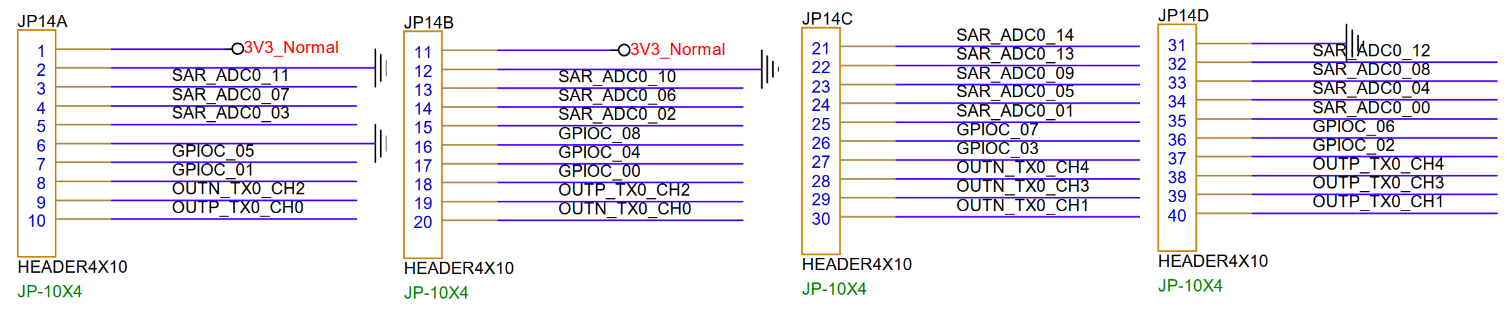
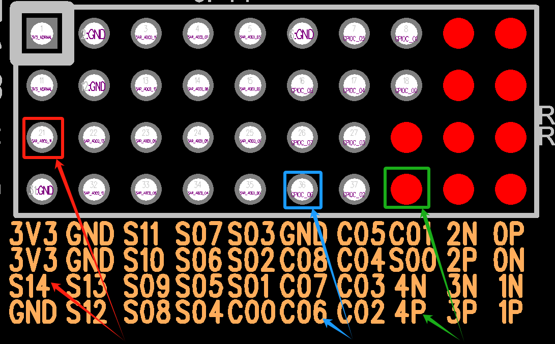
This section of IO is reserved for pin headers, and can be configured for other functions as needed, such as TTL screens. Supported functions can be found in the HW checklist of ARM Tmux. The front of the PCB can identify pin header network names based on the silkscreen. For example, S14 is SAR_ADC_14, C06 is GPIOC_06, 4P is OUTP_TX0_CH4.
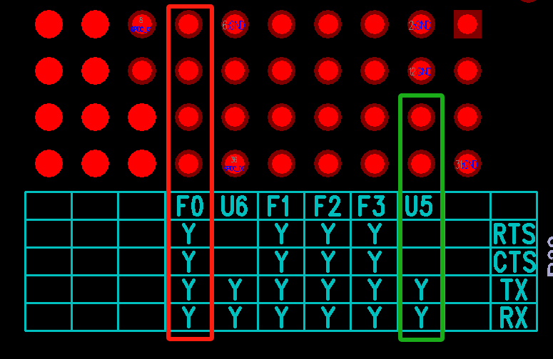
The back of the PCB can identify UART and FUART interfaces based on the silkscreen. For example, F0 is FUART0, and the two pin headers correspond to RTS/CTS/TX/RX from top to bottom. U5 is UART5, and the two pin headers below correspond to TX/RX from top to bottom.
3.25. ETH and Sensor Control Selection (JP185)
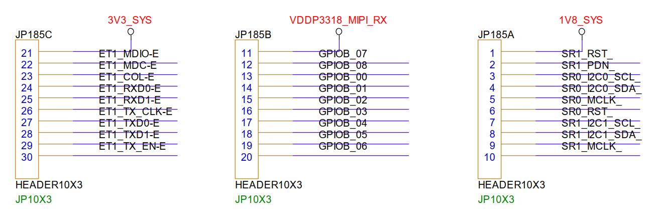
Due to IO allocation, there is a conflict with ETH1 and sensor control signals. Currently, it is selected using a jumper cap. The factory default is the sensor interface with JP185 fully connected to A-B, and if ETH1 is needed, JP185 jumper caps must be connected completely to B-C.
Note: To enable ETH1, the dts configuration needs to be modified. For specifics, you can refer to the DTS node enabling EMAC1 example
3.26. EMMC(UEM1)
EMMC supports EMMC5.0, HS200/400 by default. Note: EMMC and SD interfaces share a power domain, the default voltage for EMMC is 1.8V. At this time, the SD1 TF interface cannot use a TF card but can use 1.8V SDIO Wifi.
3.27. SAR TEST(JP15)
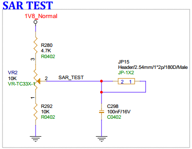
The board has a reserved sliding rheostat for SAR testing, which can be pulled to other SAR ports for validation, and adjust voltage using VR2.
3.28. SR MIPI RX 1lane(J6)
J6 connects to a 1Lane MIPI Sensor.
3.29. SR MIPI RX 2lane(J5)
J5 is default connected to a 1lane MIPI Sensor, but can also connect to a 2lane MIPI Sensor; when connecting to a 2lane MIPI Sensor, there is a multiplexing relationship between J6 and J5 (CH2P/N) and both cannot be used together. When connecting to a 1lane MIPI sensor, J6 and J5 can be used simultaneously.
3.30. DMIC(J8/J9)
J8 is for 4Ch DMIC, supporting up to 8 DMICs; J9 is for 2Ch DMIC, supporting up to 4 DMICs; there is a multiplexing relationship between J8 and J9, D2/D3 cannot be used simultaneously, after using D2/D3 on J9, J8 can only connect to D0/D1 for 2ch.
3.31. TF Card Slot (SD1)
The TF card slot is designed considering connection with SDIO WIFI, which can support 1.8V. When connecting an external TF card, because the TF card slot and eMMC share a power domain, the default is 1.8V, and the TF card does not support a signal level fixed at 1.8V. Therefore, using a TF card requires R77 to be NC, and R76 to be installed with 0R; if using both TF card and eMMC simultaneously, please NC R77 and REM37, and install R76 and REM41 with 0R, at which time EMMC can only run EMMC4.3 protocol.

3.32. KEY PAD (JP16)
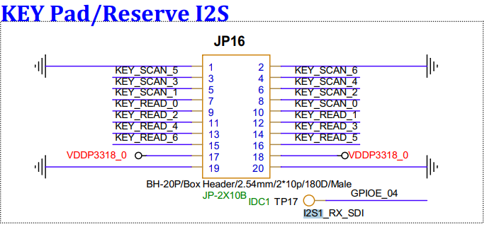
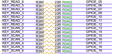
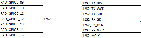
Reserved KEY PAD interface, can be used for connecting a matrix keyboard or I2S; when connecting a matrix keyboard, it cannot be shared with IR and ETH.
3.33. PM_IR(IR5)
IR reception interface for RISCV.
3.34. IR1 2 3 4(IR1 2 3 4)
IR reception interface for ARM, not yet mounted by default.
3.35. ETH0(CONR1)
CONR1 is the ETH0 100Mbps ethernet interface 0.
3.36. ETH1(CONR2)
CONR2 is the ETH1 100Mbps ethernet interface 1.
Note
Note: By default, it is not available; JP185 jumper caps need to be entirely changed to B-C.