Gpio_DebugSop
REVISION HISTORY
| Revision No. | Description |
Date |
|---|---|---|
| 1.0 | 12/19/2024 |
Introduction
This document is written for FAE and software development personnel, aiming to introduce how to conduct preliminary troubleshooting when customers encounter GPIO-related issues during the development process, and to provide relevant information to RD for analysis after confirming it is a Sigmastar issue.
1. Common Basic Operations and Commands for Debugging
1.1 echo Command
Supports userspace to apply for GPIO, configure level modes, query multiplexing function conflicts, and other operations through the echo command. For details, see GPIO Usage Reference Chapter 4.3.
1.2 HW Checklist Instructions Related to GPIO Usage
This section mainly explains the linkage between the GPIO part in the HW checklist and the riu_r/w instructions.
1.2.1 Configuration Instructions
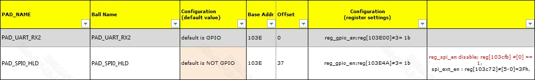
The HW checklist includes all pins that can be used as GPIO, with information about the pins in the table, including default pin status, input register address, output register address, drive capability adjustment register address, pull-up register address, pull-down register address, etc. The following illustrations are for example purposes only; specific register configurations should refer to the corresponding platform release files.
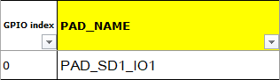
GPIO index and PAD_NAME are the most basic information about the pin, representing the GPIO index number and name, respectively.
Configuration (register settings) indicates the registers that need to be operated to set the pin as GPIO MODE. For example, if this pin is to be used as GPIO, BIT3 in register [103E3C] needs to be written as 1, which will be referred to as con_bit below.
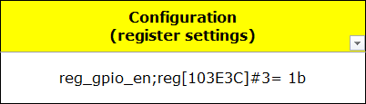
reg[103E3C] indicates that the Bank Addr of the register to be operated is 0x103E, and the Offset Addr is (0x3C) / 2 = 0x1E.
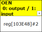
OEN indicates the direction register of the pin in GPIO MODE, where 0 indicates output and 1 indicates input. For example, it indicates that BIT2 in register [103E48] needs to be checked, which will be referred to as oen_bit below.
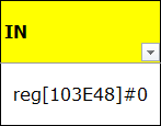
IN indicates the level value of GPIO in input mode, where 0 indicates low level and 1 indicates high level. For example, it indicates that BIT0 in register [103E48] needs to be checked, which will be referred to as in_bit below.
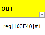
OUT indicates the level value of GPIO in output mode, where 0 indicates low level and 1 indicates high level. For example, it indicates that BIT1 in register [103E48] needs to be checked, which will be referred to as out_bit below.
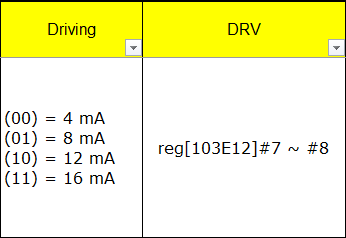
Driving and DRV indicate the driving capability information of the pin. Driving indicates the specific level of the pin's driving capability, while DRV indicates the register needed to adjust the driving capability level. For example, this pin has four driving capabilities of 4mA, 8mA, 12mA, and 16mA, which can be operated through BIT7 and BIT8 of register [103E12].
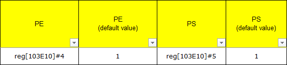
PE and PS indicate the registers needed to adjust the internal pull-up and pull-down of the pin. PE (default value) and PS (default value) indicate the default values of the corresponding registers. For example, the registers that need to be operated for adjusting the internal pull-up and pull-down of the pin are BIT4 and BIT5 of [103E10].
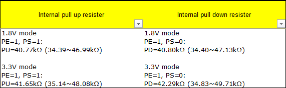
The specific values of PE and PS can be confirmed through the following two columns, where PE=1 and PS=1 indicates pull-up; PE=1 and PS=0 indicates pull-down.
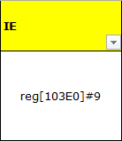
IE indicates Input-Enable, which is related to the input function of the pin. Any multiplexing function involving input needs to set this bit, and it must not be confused with OEN's input. IE is enabled by default.
1.2.2 Control GPIO State
| Step | Description |
|---|---|
| A | Obtain HW checklist |
| B | Find the Configuration (register settings) information for the pin to be operated, which provides bank, offset, and corresponding con_bit, see 1.2.1 Configuration Instructions |
| C | Find the OEN information for the pin to be operated, which provides bank, offset, and corresponding oen_bit. Generally, the bank and offset here are consistent with step B, see 1.2.1 Configuration Instructions |
| D | Find the OUT information for the pin to be operated, which provides bank, offset, and corresponding out_bit, see 1.2.1 Configuration Instructions |
| E | Find the IN information for the pin to be operated, which provides bank, offset, and corresponding in_bit, see 1.2.1 Configuration Instructions |
| F | riu_r bank offset, obtain the GPIO state of the pin before operation |
| G | Modify the corresponding bits of con_bit, oen_bit, out_bit, and in_bit based on the value obtained in step F. Note! Do not touch other bits under this offset output-high: con_bit=1, oen_bit=0, out_bit=1 output-low: con_bit=1, oen_bit=0, out_bit=0 input: con_bit=1, oen_bit=1 |
| H | Write the modified value through riu_w: riu_w bank offset value |
1.2.3 Obtain GPIO Enable Status
| Step | Description |
|---|---|
| A | Obtain HW checklist |
| B | Find the Configuration (register settings) information for the pin to be operated, which provides bank, offset, and corresponding con_bit, see 1.2.1 Configuration Instructions |
| C | riu_r bank offset, obtain the current GPIO state of the pin. If the state of con_bit matches what is described in the HW checklist, it indicates that the GPIO mode is enabled; otherwise, it is not. |
| D | To further obtain the current input/output mode and level status of the pin, continue to step E |
| E | Find the OEN information for the pin to be operated, which provides bank, offset, and corresponding oen_bit. oen_bit=1 indicates input, oen_bit=0 indicates output |
| F | Find the OUT information for the pin to be operated, which provides bank, offset, and corresponding out_bit. out_bit=1 indicates output-high, oen_bit=0 indicates output-low |
| G | Find the IN information for the pin to be operated, which provides bank, offset, and corresponding in_bit. in_bit indicates the actual external level of the current pin, so if it is found that the values of in_bit and out_bit are not equal in output mode, it indicates that the level state of this pin is abnormal. |
The Configuration (register settings) information involved in process B corresponds to only one register address for most pins, but there are cases where the pin Configuration information corresponds to multiple registers. Specific situations can be queried in the HW checklist, and the overall idea is the same, confirming whether these registers' corresponding bits are enabled.
1.2.4 Control GPIO Internal Pull-Up and Pull-Down
| Step | Description |
|---|---|
| A | Obtain HW checklist |
| B | Find the PE information for the pin to be operated, which provides bank, offset, and corresponding pe_bit, see 1.2.1 Configuration Instructions |
| C | Find the PS information for the pin to be operated, which provides bank, offset, and corresponding ps_bit, see 1.2.1 Configuration Instructions |
| D | Find the Internal pull-up register and Internal pull-down register, determine the state of PE and PS under pull-up and pull-down conditions, see 1.2.1 Configuration Instructions |
| E | riu_r bank offset, obtain the GPIO state of the pin before operation |
| F | Modify the corresponding bits of pe_bit and ps_bit based on the value obtained in step E. Note! Do not touch other bits under this offset |
| G | Write the modified value through riu_w: riu_w bank offset value |
The query of GPIO pull-up and pull-down status can also follow this method.
1.2.5 Adjust GPIO Driving Capability
| Step | Description |
|---|---|
| A | Obtain HW checklist |
| B | Find the DRV information for the pin to be operated, which provides bank, offset, and corresponding drv_bit[m,n], see 1.2.1 Configuration Instructions |
| C | Find the Driving information for the pin to be operated, which provides the current driving capability level supported by the pin |
| D | riu_r bank offset, obtain the GPIO state of the pin before operation |
| E | Based on the value obtained in step D, write the desired driving capability level into the corresponding bits of drv_bit[m,n]. Note! Do not touch other bits under this offset |
| F | Write the modified value through riu_w: riu_w bank offset value |
The query of the current driving capability of GPIO can also follow this method.
1.3 Tmux_Table Usage Instructions
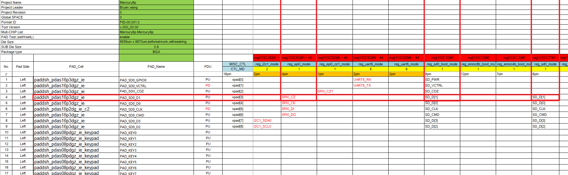
Tmux_Table is a summary of all multiplexing functions. When it is necessary to set a specific multiplexing function for a pin, you can refer to this table to find the specific bank, offset, and bit that need to be operated.
1.3.1 Register Configuration for Multiplexing Functions
The following illustration explains the steps for operating the multiplexing function registers.
| Step | Description |
|---|---|
| A | Obtain Tmux_Table |
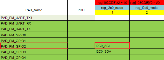
| B | Find the pin to be operated: PAD_PM_GPIO2, the multiplexing function to be set: I2C0_SCL |
| C | After horizontal and vertical positioning, you can see that the register to be operated is reg[103CDE]#2~#0, confirming bank: 103C offset: DE/2=6F bit[2:0] |
| D | Query the number of modes below the same column as reg[103CDE]#2~#0, i.e., the yellow background position in the figure, which is 1, indicating that bit[2:0] should be written as 1 |
| E | riu_r bank offset, obtain the value of this register |
| F | Based on the value obtained in step D, modify the value of bit[2:0] to 1. Note! Do not touch other bits under this offset |
| G | Write the modified value through riu_w: riu_w bank offset value |
The query of the current multiplexing function of the pin can also follow this method.
1.3.2 Multiplexing Function Conflict Check
Method 1 (Using Tmux_Table):
| Step | Description |
|---|---|
| A | Obtain Tmux_Table |
| B | Find the corresponding row of the pin to be queried in Tmux_Table |
| C | According to the method mentioned in 1.3.1, confirm the enable status of all multiplexing functions of this pin |
| D | According to the method mentioned in 1.2.3, confirm the enable status of the GPIO mode of this pin |
| E | After all function queries are completed, you can determine whether multiple multiplexing functions are enabled at present. |
Method 2 (Using drivers/sstar/gpio/chip_name/hal_pinmux.c):
| Step | Description |
|---|---|
| A | Enter hal_pinmux.c |
| B | Find the array corresponding to the pin to be queried, which contains the relevant macro definitions for setting multiplexing functions: bank offset mask value |
| C | Query the multiplexing functions from top to bottom in the array |
| D | After all multiplexing function queries are completed, you can determine whether multiple multiplexing functions are enabled at present. |
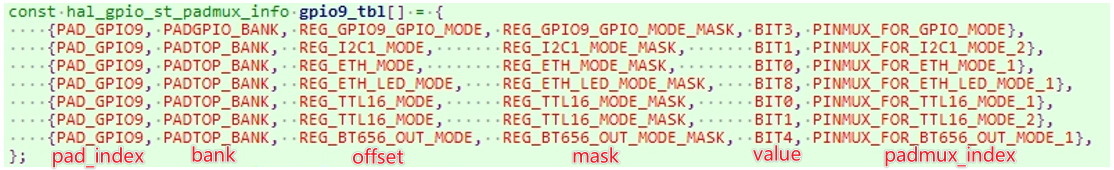
For example, if you want to check whether I2C1_MODE_2 is enabled for the current pin, you can find in the code:
#define PAD_GPIO9 17

#define PADTOP_BANK 0x103C00

#define REG_I2C1_MODE      0x53
#define REG_I2C1_MODE_MASK BIT0 | BIT1

#define BIT1  0x02

#define PINMUX_FOR_I2C1_MODE_2 0x12
Therefore, you need to pay attention to whether the value of bank: 0x103C offset:0x53's bit[1:0] is 0x2, that is, whether BIT0=0 and BIT1=1. If so, it indicates that I2C1_MODE_2 is currently enabled.
hal_pinmux.c summarizes all the multiplexing functions supported by all pins, which is more intuitive than querying Tmux_Table, as it allows direct access to the registers of the multiplexing functions supported by the pin.
Method 3 (Using /sys/devices/virtual/sstar/msys/mux_verify node for confirmation):
| Step | Description |
|---|---|
| A | Open OCNFIG: CONFIG_MSYS_PADMUX when compiling the kernel |
| B | For usage, see the conflict check of multiplexing functions in 1.1 |
2. Common Problem Analysis
2.1 Abnormal Level Control
Refer to the following debug flowchart.
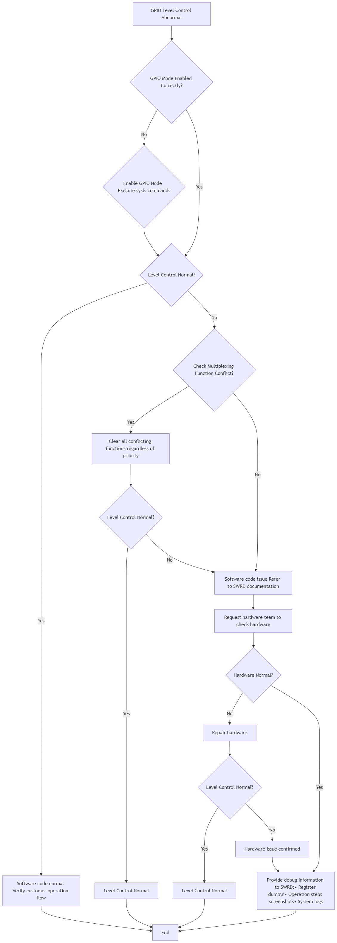
Flowchart Explanation: For determining whether the GPIO mode is correctly enabled, refer to 1.2.3 Obtain GPIO Enable Status. For determining whether there are conflicts in multiplexing functions, refer to 1.3.2 Multiplexing Function Conflict Check. Provide register information to SWRD, including PADTOP BANK (0x103C) and PADGPIO BANK (0x103E).
2.2 Configured Multiplexing Function Not Effective
Refer to the following debug flowchart.
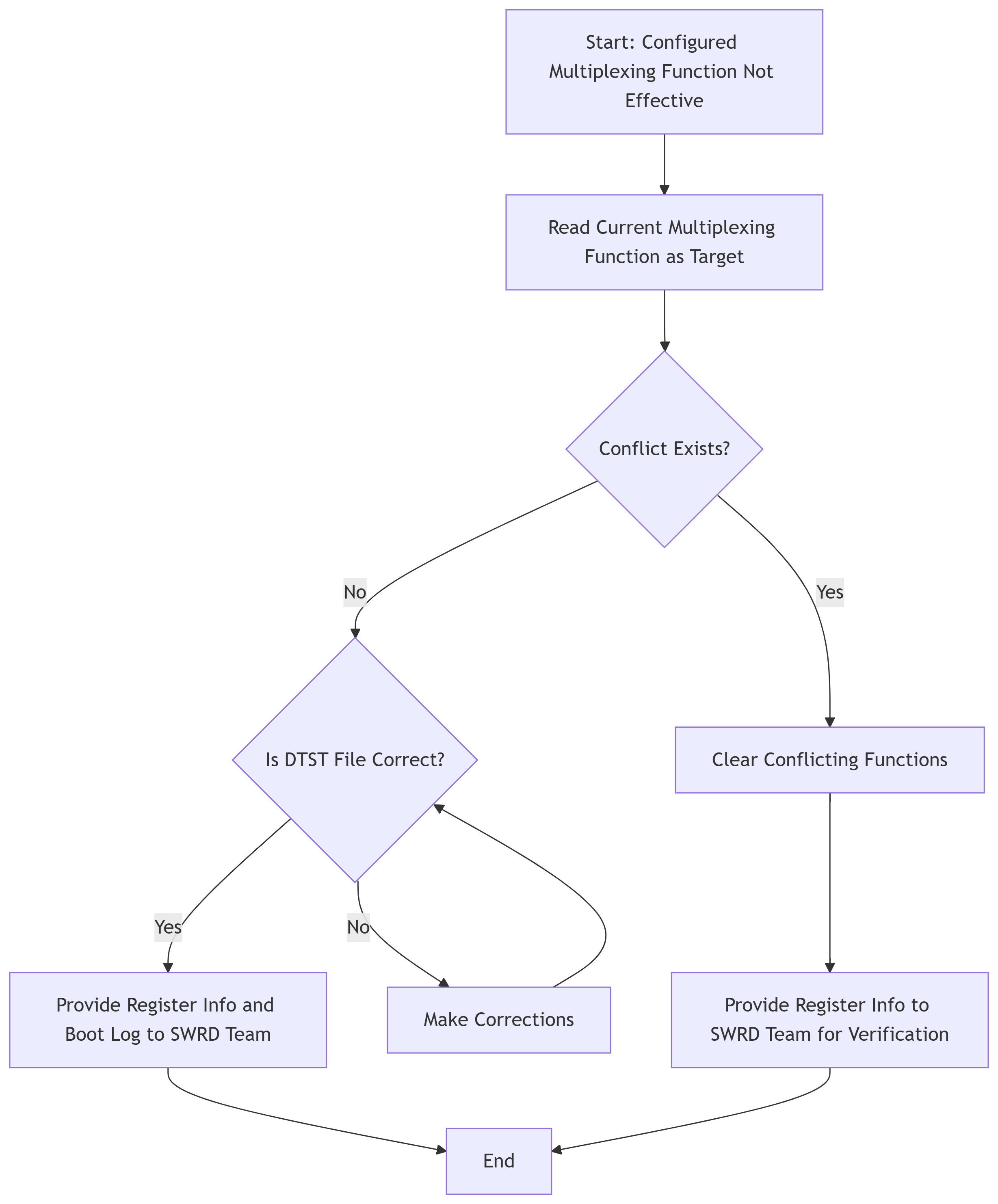
Flowchart Explanation: Confirm that the dtsi file for configuring the multiplexing function is correct. You can add mandatory error codes in the configuration file for compilation. If an error occurs, it indicates that the selected configuration file is correct; if no error occurs, it indicates that the configuration file is incorrect. For determining whether there are conflicts in multiplexing functions, refer to 1.3.2 Multiplexing Function Conflict Check. Provide register information to SWRD, including PADTOP BANK (0x103C) and PADGPIO BANK (0x103E).