SENSOR USER GUIDE
REVISION HISTORY
| Revision No. | Description |
Date |
|---|---|---|
| 1.0 | 11/19/2025 |
1. OVERVIEW
This article takes the Comake_Pi_D2 development board of the IFORD series chips as an example to provide a reference for the use of image sensors. It is necessary to understand some basic technical knowledge, including the CSI interface and CCI interface in the MIPI protocol, as well as the specifications of the sensor.
To ensure that the image sensor outputs images correctly, please follow these steps:
- Confirm that the hardware connection between the sensor and the SOC chip is correct.
- Identify which pins on the SOC chip can be used for the sensor's MIPI interface.
- Properly configure the CSI and sensor_if interface parameters in the device tree (dts).
- Confirm the module KO files that need to be loaded.
- Confirm the sensor driver KO files that need to be loaded.
- Correctly use the API interfaces of the MI module.
2. KEYWORD
- sensor : Refers to the sensor. In embedded audio and video development, when "sensor" is mentioned separately, it specifically refers to CMOS image sensors, which function to capture image data.
- sensor pad : Refers to the pins on the SoC chip that correspond to the sensor hardware.
- mipi : Refers to the MIPI protocol suite, which includes protocols for touch, image capture, image display, etc. In the context of sensor usage, "mipi" specifically refers to the CSI-2 protocol/interface (a type of image capture protocol); in panel or display scenarios, "mipi" specifically refers to the DSI protocol/interface (a type of image display protocol).
- lane : An abstract concept for actual physical wiring, referred to as a "channel." For example, there are clock lanes (clock lane) and data lanes (data lane). A single lane corresponds to one or more physical wires. For example, in the physical layer D-PHY of the CSI-2 protocol in the MIPI protocol suite, a single data lane consists of two physical wires: "data-" and "data+." Some sensors support multiple data lanes, such as the GC2053 sensor, which is equipped with 2 data lanes (based on D-PHY), corresponding to 4 physical data lines. By default, when "lane" is mentioned separately, it refers to the "data channel."
3. FUNCTIONAL DESCRIPTION
The sensor padmux configuration provides the necessary reset and power down pin voltages for sensor power-up and power-down sequences, ensuring compliance with the sensor's required timing. Additionally, it enables I2C pin configuration between the master and slave devices for reading/writing sensor registers.The sensor padmux supports multiple modes, including MIPI mode, and others. By modifying the active mode, the corresponding pins can be used to transmit data into the IC.
-
Different chips support varying MCLK frequencies. The MCLK frequencies supported by iford are as follows:
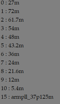
supported mclk frequency
4. HARDWARE CONNECTION OVERVIEW
4.1. HARDWARE INTERFACE CONFIRMATION
Note:
Iford supports a maximum specification of MIPI0 (4 lanes). MIPI0 can be split into MIPI00 and MIPI01 -- snr00 and snr01.
The Iford series MIPI 4-lane supports the connection of 4-lane sensors and is also compatible with 2-lane sensors. MIPI 2-lane supports the connection of 2-lane sensors and is also compatible with 1-lane sensors. The accompanying sensor IMX681 for the Comake_Pi_D2 is a 2-lane sensor. Below, we will use the Comake_Pi_D2 and IMX681 sensor as an example.
Confirm which pins on the SOC chip are connected to the sensor
4-lane MIPI mode:
The schematic diagram for the 4-lane connection of snr0 on the Comake_Pi_D2 is shown below. The 4-lane configuration is compatible with 2-lane. As illustrated, snr0 is connected to the SJ6 connector:
- "681_D0P/N", "MIPI_D0P/N", and "PAD_OUTP/N_RX0_CH[1]" are connected.
- "681_D1P/N", "MIPI_D1P/N", and "PAD_OUTP/N_RX0_CH[0]" are connected.
- "681_CKP/N", "MIPI_CKP/N", and "PAD_OUTP/N_RX0_CH[2]" are connected.
- "471_D2N/P", "MIPI_D2P/N", and "PAD_OUTP/N_RX0_CH[3]" are connected.
-
"471_D3N/P", "MIPI_D3P/N", and "PAD_OUTP/N_RX0_CH[4]" are connected.
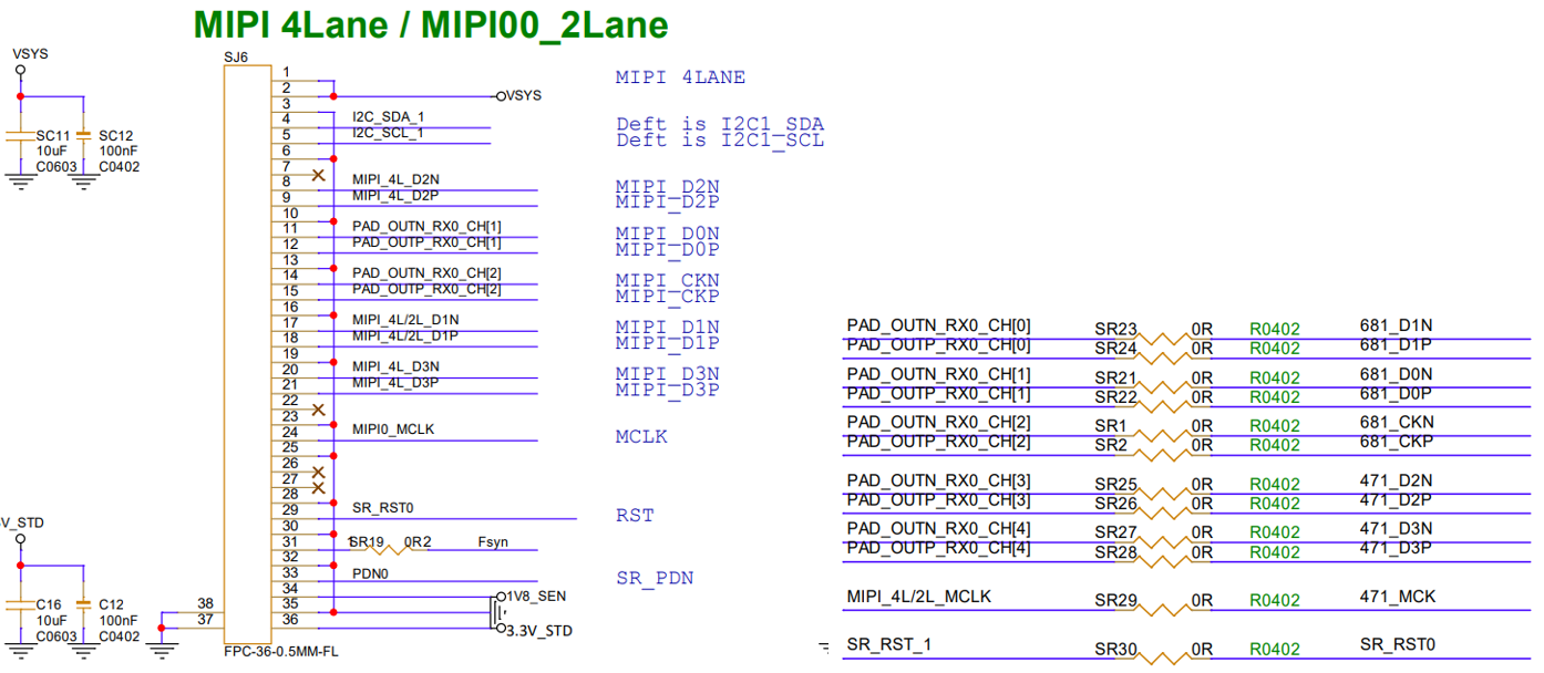
From the above, we can summarize the corresponding table as follows:
| MIPI | PAD |
|---|---|
| MIPI_D0N/P (data0 lane) | PAD_OUTN/P_RX0_CH[1] |
| MIPI_D1N/P (data1 lane) | PAD_OUTN/P_RX0_CH[0] |
| Clock lane (MIPI_CKP) | PAD_OUTN/P_RX0_CH[2] |
| MIPI_D2N/P (data2 lane) | PAD_OUTN/P_RX0_CH[3] |
| MIPI_D3N/P (data3 lane) | PAD_OUTN/P_RX0_CH[4] |
Based on the hardware schematic and by referring to the HW Checklist, it can be determined from the table above that the current snr0 MIPI mode is set to mode 5.
If the connected sensor is a 4-lane sensor, you can refer to the MIPI pinmux table to correctly connect the actual MIPI to RX_CH. According to the subsequent description of the MIPI wiring sequence, just configure the correct wiring sequence.
2+2 lane MIPI mode
The schematic diagram for snr01 in 2-lane mode on the Comake_Pi_D2 is shown below. The 2-lane wiring sequence is compatible with the 4-lane configuration. The 2-lane schematic for snr00 can be referred to from the 4-lane schematic mentioned above. The connection method for snr01 in 2-lane mode is as follows:
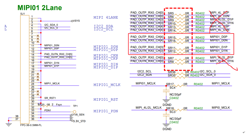
snr01 is connected to the SJ1 connector:
- "MIPI01_D0P/N" is connected to "PAD_OUTP/N_RX0_CH[4]".
- "MIPI01_D1P/N" is connected to "PAD_OUTP/N_RX0_CH[3]".
- "MIPI01_CKP/N" is connected to "PAD_OUTP/N_RX0_CH[5]".
From the above, we can summarize the corresponding table as follows:
| MIPI | PAD |
|---|---|
| MIPI_D0N/P (data0 lane) | PAD_OUTN/P_RX0_CH[1] |
| MIPI_D1N/P (data1 lane) | PAD_OUTN/P_RX0_CH[0] |
| Clock lane (MIPI_CKP) | PAD_OUTN/P_RX0_CH[2] |
| MIPI01_D0N/P (data0 lane) | PAD_OUTN/P_RX0_CH[4] |
| MIPI01_D1N/P (data1 lane) | PAD_OUTN/P_RX0_CH[3] |
| Clock lane (MIPI01_CKP/N) | PAD_OUTN/P_RX0_CH[5] |
Based on the hardware schematic and referring to the HW Checklist, as per the above table for MIPI pinmux, the current MIPI mode is selected as mode 5.
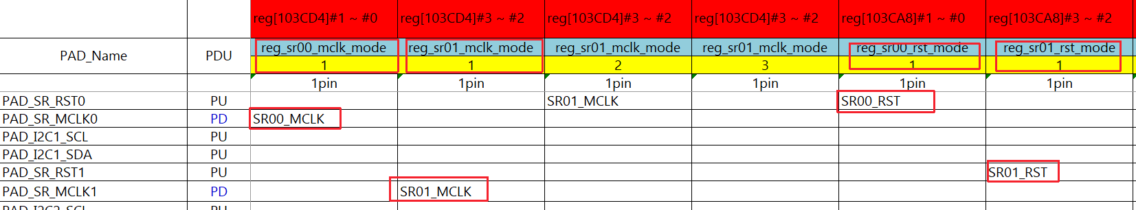
mclk_mode and rst_mode
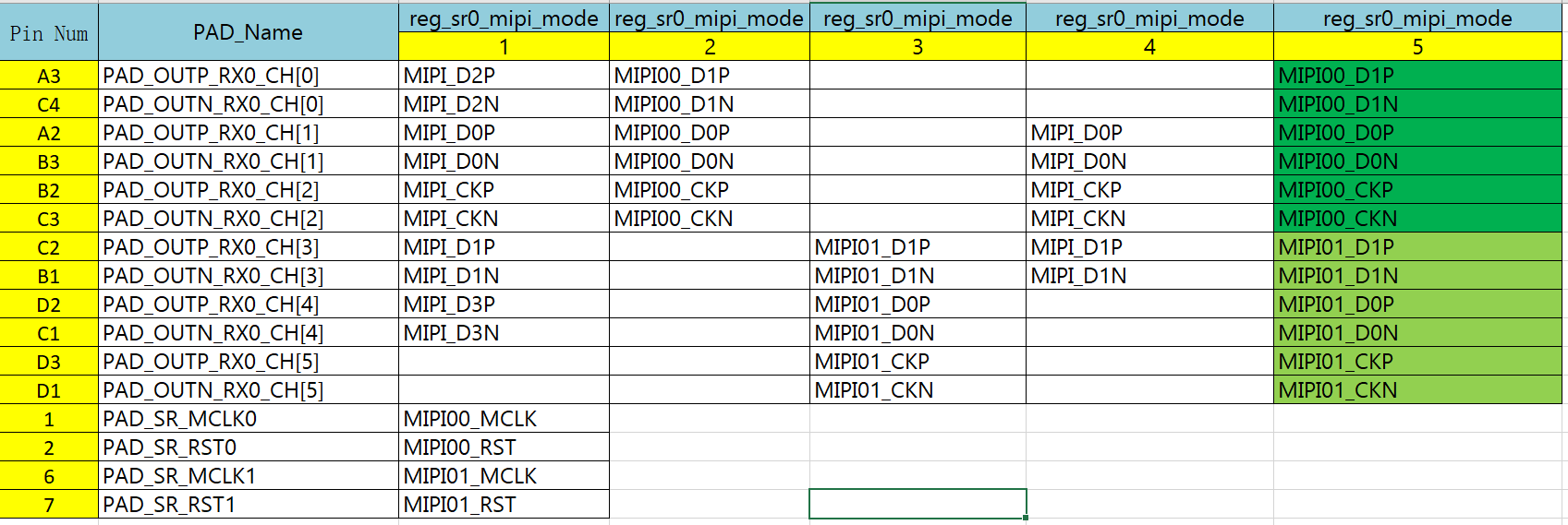
By consulting the MIPI pinmux and PAD_list tables from the HW Checklist, as shown in Figure 4-2 MIPI Pinmux and the figure below, we can determine the following:
mclk_mode
In the case of 4-lanes, mipi_mode = 1. In the case of 2+2 lanes, snr00 mipi_mode = 1 and snr01 mipi_mode = 1.
rst_mode
In the case of 4-lanes, rst_mode = 1. In the case of 2+2 lanes, snr00 rst_mode = 1 and snr01 rst_mode = 1.
pdn_mode
PDN is actually used to control the sensor power down. By writing different values to the registers reg_sr00_pdn_mode and reg_sr01_pdn_mode, the SOC's external sensor PDN pins will also differ. The dts uses the configuration item snr_sr0_mipi_pdn_mode to pass values to the reg_sr00_pdn_mode register. It is essential to note that some sensor PDN pins can be left floating and do not require control. The PDN on the Comake_Pi_D2 board is already connected to the SOC but is not used by default. The specific connection situation can be checked in the hardware schematic.
When configuring the reg_mipi_rx_mode, reg_mclk_mode, reg_rst_mode, and reg_i2c_mode registers for snr0 and snr2 with different values, there are various applications. The reg_i2c_mode can refer to the 5.2 IIC Configuration section of this article. Below is a recommended usage combination.
| Panmux Mode Type | 4Lane | 2+2Lane |
|---|---|---|
| Pad Num | snr0 | snr0 & snr2 |
| mipi_rx_mode | mode5 | mode5 & mode5 |
| mclk_mode | mode1 | mode1 & mode1 |
| rst_mode | mode1 | mode1 & mode1 |
| I2C_BUS | I2C1 | I2C1 & I2C2 |
4.2. MIPI Interface Wiring Sequence Matching
In the DTS, the MIPI wiring sequence can be configured through csi_sr0_lane_select, and the P/N swap of the MIPI wiring sequence can be configured through csi_sr0_lane_pn_swap. The configuration methods for csi_sr0_lane_select and csi_sr0_lane_pn_swap are shown below. Please configure the correct MIPI wiring sequence according to the actual hardware connections.
csi_sr0_lane_select = < CLK, DataLane0, DataLane1, DataLane2, DataLane3>

csi_sr0_lane_pn_swap = < CLK, DataLane0, DataLane1, DataLane2, DataLane3>

# Where CLK, DataLane0, DataLane1, etc. are relative positions.
Next, we will take the 4-lane and 2+2 lane as examples to detail the usage of csi_sr0_lane_select and csi_sr0_lane_pn_swap.
4-lane:
From the 4.1 Hardware Connection Introduction section's 4-lane description, the corresponding sensor pad matching relationship is represented in the following table:
| MIPI | PAD |
|---|---|
| MIPI_D0N/P (data0 lane) | PAD_OUTN/P_RX0_CH[1] |
| MIPI_D1N/P (data1 lane) | PAD_OUTN/P_RX0_CH[0] |
| Clock lane (MIPI_CKP) | PAD_OUTN/P_RX0_CH[2] |
| MIPI_D2N/P (data2 lane) | PAD_OUTN/P_RX0_CH[3] |
| MIPI_D3N/P (data3 lane) | PAD_OUTN/P_RX0_CH[4] |
Thus, csi_sr0_lane_select = <2 1 0 3 4>.
If the MIPI data lane P/N is reversed, then the polarity in the above table needs to be set with csi_sr0_lane_pn_swap = <1 1 1 1 1>.
2+2 lane:
From the 4.1 Hardware Connection Introduction section's 2+2 lane description, the corresponding sensor pad matching relationship is represented in the following table:
| Sensor | MIPI | PAD |
|---|---|---|
| snr00 | MIPI_D0N/P (data0 lane) | PAD_OUTN/P_RX0_CH[1] |
| snr00 | MIPI_D1N/P (data1 lane) | PAD_OUTN/P_RX0_CH[0] |
| snr00 | Clock lane (MIPI_CKP) | PAD_OUTN/P_RX0_CH[2] |
| snr01 | MIPI01_D0N/P (data0 lane) | PAD_OUTN/P_RX0_CH[3] |
| snr01 | MIPI01_D1N/P (data1 lane) | PAD_OUTN/P_RX0_CH[4] |
| snr01 | Clock lane (MIPI01_CKP/N) | PAD_OUTN/P_RX0_CH[5] |
For MIPI00 2-lane (snr00):
csi_sr0_lane_select = <2 1 0>
If the MIPI data lane P/N is reversed, then it needs to be set with csi_sr0_lane_pn_swap = <1 1 1>.
For MIPI01 2-lane (snr01):
Note: The CLK, DataLane0, DataLane1, etc. in csi_sr0_lane_select are relative positions, so
csi_sr2_lane_select = <2 1 0>.
If the MIPI data lane P/N is reversed, then it needs to be set with csi_sr2_lane_pn_swap = <1 1 1>.
Quick Method to Confirm Lane Wiring Sequence Modification:
# Read the register to confirm that the lane order modification is effective.

/customer/riu_r 0x1538 # Read 0x6 0xA 0xE 0x22 0x25 to check if the order has taken effect.

# 0x1538 is for sensor0.

# 0x153C is for sensor2.
Quick Method to Modify Lane Wiring Sequence:
Since modifying the sensor wiring sequence requires replacing the kernel, which is cumbersome, you can first use the following method to quickly change the wiring sequence by loading:insmod /config/modules/5.10/mi_sensor.ko gp_sntExternalConfig=/customer/sensorpad0_2lane.json
For example:
IMX681 2-lane wiring sequence 2 1 0:
    {
        "SensorIF": [
            {
                "sensorPad": 0,
                "hwClass": "mipi",
                "content": {
                    "lane_number": 2,
                    "hdr_lane_number": 2,
                    "lane_select": "2,1,0",
                    "lane_swap": "0,0,0"
                }
            }
        ]
    }
5. KERNEL USAGE GUIDE
5.1. DTS CONFIGURATION
4lane:
    csi: csi {
                compatible = "sgs,csi";
                io_phy_addr = <0x1f000000>;
                banks = <0x153C>,<0x153D>,<0x153E>,<0x1538>,<0x153A>,<0x153B>;
                atop_banks = <0x153F>;
                clkgen_banks = <0x1038>;
                interrupts=  <GIC_SPI INT_IRQ_MIPI_CSI2 IRQ_TYPE_LEVEL_HIGH>;
                clocks = <&CLK_csi0_mac_lptx_top_i>,<&CLK_csi0_mac_top_i>,<&CLK_csi0_ns_top_i>,<&CLK_csi1_mac_lptx_top_i>,<&CLK_csi1_mac_top_i>,<&CLK_csi1_ns_top_i>;
                status = "ok";
                /* Config max lane number */
                csi_sr0_lane_num = <4>;
                /* Config lane selection */
                csi_sr0_lane_select = <2 1 3 0 4>;
                /* Config lane P/N swap */
                csi_sr0_lane_pn_swap = <1 1 1 1 1>;
            };
    sensorif: sensorif {
                compatible = "sgs,sensorif";
                status = "ok";
                clocks = <&CLK_sr00_mclk>, <&CLK_sr01_mclk>;

                /* Config sensor 0 pad mux */
                snr_sr0_mipi_mode         = <1>;
                snr_sr0_mipi_rst_mode     = <1>;
                snr_sr0_mipi_pdn_mode     = <0>;
                snr_sr0_mipi_mclk_mode    = <1>;
                snr_sr0_rst_gpio          = <-1>;
                snr_sr0_pdn_gpio          = <-1>;

                /* Config mclk 37.125MHz supported */
                snr_sr0_mclk_37p125 = <1>;

                /* Config i2c for sensor pad */

                snr0_mipi_i2c = <0>;
            };
2+2lane:
    csi: csi {
                compatible = "sgs,csi";
                io_phy_addr = <0x1f000000>;
                banks = <0x153C>,<0x153D>,<0x153E>,<0x1538>,<0x153A>,<0x153B>;
                atop_banks = <0x153F>;
                clkgen_banks = <0x1038>;
                interrupts=  <GIC_SPI INT_IRQ_MIPI_CSI2 IRQ_TYPE_LEVEL_HIGH>;
                clocks = <&CLK_csi0_mac_lptx_top_i>,<&CLK_csi0_mac_top_i>,<&CLK_csi0_ns_top_i>,<&CLK_csi1_mac_lptx_top_i>,<&CLK_csi1_mac_top_i>,<&CLK_csi1_ns_top_i>;
                status = "ok";
                /* Config max lane number */
                csi_sr0_lane_num = <2>;
                csi_sr2_lane_num = <2>;
                /* Config lane selection */
                csi_sr0_lane_select = <2 1 0 3 4>;
                csi_sr2_lane_select = <2 1 0>;
                /* Config lane P/N swap */
                csi_sr0_lane_pn_swap = <0 0 0 0 0>;
                csi_sr2_lane_pn_swap = <0 0 0>;
            };
    sensorif: sensorif {
                compatible = "sgs,sensorif";
                status = "ok";
                clocks = <&CLK_sr00_mclk>, <&CLK_sr01_mclk>;

                /* Config sensor 0 pad mux */
                snr_sr0_mipi_mode         = <1>;
                snr_sr0_mipi_rst_mode     = <1>;
                snr_sr0_mipi_pdn_mode     = <0>;
                snr_sr0_mipi_mclk_mode    = <1>;
                snr_sr0_rst_gpio          = <-1>;
                snr_sr0_pdn_gpio          = <-1>;

                /* Config sensor 2 pad mux */
                snr_sr2_mipi_mode         = <1>;
                snr_sr2_mipi_rst_mode     = <1>;
                snr_sr2_mipi_pdn_mode     = <0>;
                snr_sr2_mipi_mclk_mode    = <1>;
                snr_sr2_rst_gpio          = <-1>;
                snr_sr2_pdn_gpio          = <-1>;

                /* Config mclk 37.125MHz supported */
                snr_sr0_mclk_37p125 = <1>;
                snr_sr2_mclk_37p125 = <1>;

                /* Config i2c for sensor pad */
                snr0_mipi_i2c = <1>;
                snr2_mipi_i2c = <2>;
            };
The definitions of the CSI section are as follows:
The meanings of the CSI parameters are as follows:
| Parameter | Meaning | Remarks |
|---|---|---|
| interrupts | MIPI RX CSI interrupt | No modification needed |
| clocks | MIPI RX CSI clock source | No modification needed |
| csi_sr0_lane_num | Configure the initialization number of snr0 data lanes | Initialize as needed; snr0 can have a maximum of four data lanes, selectable values are 0, 1, 2, 3, 4. Note: here, lane_num needs to be less than or equal to the lane count specified by the reg_mipi_mode register. If snr0 is initialized for 4 lanes, it can actually use only 4 lanes during operation. |
| csi_sr0_lane_select | Configure the relative lane order of the CSI interface snr0 | <relative_order_of_clk_lane relative_order_of_data0_lane relative_order_of_data1_lane>. The relative order refers to comparing the CH values of clk_lane, data0_lane, and data1_lane, where the smallest CH value has a relative order of 0, the middle one is 1, and the largest is 2. For example, when csi_sr0_lane_num=2, and referring to the SJ6-snr0 wiring table mentioned earlier, if clk_lane is connected to CH2 and data0_lane is connected to CH1 and data1_lane to CH0, then csi_sr0_lane_select=<2 1 0>. |
| csi_sr0_lane_pn_swap | Configure whether the polarity of snr0 lanes is reversed | <clk_lane_polarity_swap_flag data0_lane_polarity_swap_flag data1_lane_polarity_swap_flag>. There are only two reversal flag values: 0 and 1. A value of 0 indicates that the lane polarity has not been reversed, meaning N lines connect to N lines and P lines connect to P lines. A value of 1 indicates that the lane polarity has reversed, meaning N lines connect to P lines and P lines connect to N lines. This is a chip compatibility design to prevent errors in external circuit designs. You can change this configuration here. For the Comake_Pi_D2 board, the polarity of all lanes of snr0 and all lanes of snr2 have not been reversed. For example, csi_sr0_lane_pn_swap=<0 0 0>. |
| csi_sr2_lane_num | Configure the initialization number of snr2 data lanes | Initialize as needed; snr2 can have a maximum of 2 data lanes, selectable values are 0, 1, 2. |
| csi_sr2_lane_select | Configure the relative lane order of the CSI interface snr2 | Same analysis as above. |
| csi_sr2_lane_pn_swap | Configure whether the polarity of snr2 lanes is reversed | Same analysis as above; polarity is not reversed, for example, csi_sr2_lane_pn_swap=<0 0 0>. |
The definitions of the sensorif section are as follows:
| Parameter | Meaning | Remarks |
|---|---|---|
| clocks | Sensor mclk clock source | Needs to be configured according to the order of snr0 and snr2. |
| snr_sr0_mipi_mode | MIPI mode for snr0; different modes mainly correspond to different CSI interface pads (pins) | Refer to the ARMTmux sub-table in the hw_checklist. |
| snr_sr0_mipi_rst_mode | Reset mode for snr0 when using the MIPI interface; different modes mainly correspond to pad (pin) differences | Refer to the ARMTmux sub-table in the hw_checklist. |
| snr_sr0_mipi_pdn_mode | PDN mode for snr0 when using the MIPI interface; different modes mainly correspond to pad (pin) differences | Refer to the ARMTmux sub-table in the hw_checklist. |
| snr_sr0_mipi_mclk_mode | MCLK mode for snr0 when using the MIPI interface; different modes mainly correspond to pad (pin) differences | Refer to the ARMTmux sub-table in the hw_checklist. |
| snr_sr0_rst_gpio | Reset GPIO pin index for snr0 | If both rst mode and rst GPIO are configured, the GPIO setting takes precedence. |
| snr_sr0_pdn_gpio | PDN GPIO pin setting for snr0 | If both pdn mode and pdn GPIO are configured, the GPIO setting takes precedence. |
| snr_sr0_mclk_37p125 | Configure snr0 to support 37.125 MHz | 1 - supports 37.125 MHz. |
| snr0_mipi_i2c | I2C bus ID configured for snr0 | Needs to be configured according to the actual I2C bus being used. |
5.2. IIC CONFIGURATION
As shown in the previous section: In the case of 4lane, snr0 is bound to i2c1 mode1. In the case of 2+2lane, snr00 and snr01 are bound to i2c1 mode1 and i2c2 mode1.
    snr0_mipi_i2c = <1>;
    snr2_mipi_i2c = <2>;
snr0 stands for MIPI sensor 0
<1> stands for using I2C bus 1
I2C padmux is configured in the dtsi corresponding to padmux under kernel\arch\arm64\boot\dts\sgs:
    //I2C1 Mode1,sensorif_mipi_grp1_i2c
            <PAD_GPIOB_00            PINMUX_FOR_I2C0_MODE_1           MDRV_PUSE_I2C1_SCL>,
            <PAD_GPIOB_01            PINMUX_FOR_I2C0_MODE_1           MDRV_PUSE_I2C1_SDA>,
    //I2C2 Mode1,sensorif_mipi_grp0_i2c
            <PAD_GPIOB_04            PINMUX_FOR_I2C1_MODE_1           MDRV_PUSE_I2C2_SCL>,
            <PAD_GPIOB_05            PINMUX_FOR_I2C1_MODE_1           MDRV_PUSE_I2C2_SDA>,
I2c1: /customer/riu_r 0x103c 53 //Whether bit[0:1] is the value of the corresponding mode
I2c2: trust zone config
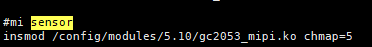
5.3. SENSOR DRIVER LOADING
5.3.1 SENSOR DRIVER CONFIGURATION
    insmod /config/modules/5.10/imx307_MIPI.ko chmap=1
    chmap mens bit map for configuration
    sensor 0 bit[0]----> chmap=1
    sensor 2 bit[2]----> chmap=4
To modify the default supported sensor drivers and pre-installed sensor drivers in the kernel, you can use the menuconfig interface.
-
enter alkaid project root directory, make menuconfig

-
press Enter to choose Sensor sub-options

-
press Enter to choose Sensor List sub-options, and write required sensor driver names

-
After editing, exit and press Enter to enter the Sensor0 submenu. Then, specify the names of the sensor drivers to be pre-loaded with insmod.

-
After completing the edits, exit and press Enter to enter the 'Sensor0 Opt' submenu. Then configure the parameters required for the pre-loaded sensor0 driver.
After compilation, the selected sensor drivers from the Sensor List will be generated under /config/modules/5.10/. Additionally, you will find the pre-configured insmod command for sensor0 in /customer/demo.sh.
5.3.2. SENSOR IQ FILE CONFIGURATION
The default sensor IQ (Image Quality) files supported by the image can be modified via menuconfig.
-
enter alkaid project root directory, make menuconfig
-
press Enter to choose Sensor sub-options
-
Press Enter to enter the IQ0 submenu, then specify the IQ file name to be used. The numerical suffix after "IQ" corresponds to different sensor pads (e.g., IQ0 maps to sensor0).
Upon successful compilation, the selected IQ file for IQ0 will be generated under /config/modules/iqfile/.
5.4. PART OF SENSOR DRIVER FUNCTION INTRODUCTION
Handle of mipi sensor interface register lists
| Parameter | Definition | Remark |
|---|---|---|
| handle->interface_attr.attr_mipi.mipi_lane_num | Register set MIPI lane number | Default : 4 |
| handle->interface_attr.attr_mipi.mipi_data_format | Register set MIPI data format | CUS_SEN_INPUT_FORMAT_YUV422, CUS_SEN_INPUT_FORMAT_RGB, |
| handle->interface_attr.attr_mipi.mipi_yuv_order | Register set MIPI yuv order | For yuv sensor only |
| handle->interface_attr.attr_mipi.mipi_hdr_mode | Register set MIPI HDR mode | CUS_HDR_MODE_NONE /No HDR/ CUS_HDR_MODE_SONY_DOL /Sony standard Line information output/ CUS_HDR_MODE_DCG /Dual Gain HDR/ CUS_HDR_MODE_EMBEEDED_RAW8 /Embedded 8bit HDR/ CUS_HDR_MODE_EMBEEDED_RAW10 /Embedded 10bit HDR/ CUS_HDR_MODE_EMBEEDED_RAW12 /Embedded 12bit HDR/ CUS_HDR_MODE_EMBEEDED_RAW14 /Embedded 14bit HDR/ CUS_HDR_MODE_EMBEEDED_RAW16 /Embedded 16bit HDR/ CUS_HDR_MODE_COMP /Compress HDR/ CUS_HDR_MODE_LI /Line Interleaved HDR/ CUS_HDR_MODE_COMP_VS /Compress HDR + very short/ CUS_HDR_MODE_VC /Virtual Channel mode/ CUS_HDR_MODE_MAX NOTE: In the old platform, CUS_HDR_MODE_DCG represented virtual channel HDR, and in the new platform it needs to rename CUS_HDR_MODE_VC. |
| handle->interface_attr.attr_mipi.mipi_hdr_virtual_channel_num | Register set HDR virtual channel number Based on each sensor VC mode header define | For example imx415: Long Exposure Frame : 0 Short Exposure Frame : 1 |
| handle->interface_attr.attr_mipi.mipi_hdr_fusion_type | Register set HDR fusion type | CUS_HDR_FUSION_TYPE_NONE,(default) CUS_HDR_FUSION_TYPE_2T1, CUS_HDR_FUSION_TYPE_3T1, |
mipi csi callback function lists
| Parameter | Definition | Remark |
|---|---|---|
| sensor_if->SetCSI_Clk (u32 idx, CUS_CSI_CLK clk) | Parameter: idx : Sensor Pad CUS_CSI_CLK : Mipi clk Set MIPI Interface MAC CLK |
Callback to CSI driver |
| sensor_if->SetCSI_Lane(u32 idx, u16 num_lane, u8 bon_off) | Parameter: idx : Sensor Pad num_lane : Mipi lane number bon_off : Enable or disable Set MIPI Interface Data Lane |
Callback to CSI driver |
| sensor_if->SetCSI_hdr_mode(idx, CUS_HDR_MODE hdr_mode, u8 bon_off) | Parameter: idx : Sensor Pad hdr_mode : bon_off : Enable or disable Set HDR Data Format |
Callback to CSI driver CUS_HDR_MODE_NONE /No HDR/ CUS_HDR_MODE_SONY_DOL /Sony standard Line information output/ CUS_HDR_MODE_DCG /Dual Gain HDR/ /Embedded 16bit HDR/ CUS_HDR_MODE_COMP /Compress HDR/ CUS_HDR_MODE_LI /Line Interleaved HDR/ CUS_HDR_MODE_COMP_VS /Compress HDR + very short/ CUS_HDR_MODE_VC /Virtual Channel mode/ CUS_HDR_MODE_MAX |
| sensor_if->SetCSI_LongPacketType(u32 idx, u16 dt0_15, u16 dt16_31, u16 u32_47) | Parameter: idx : Sensor Pad Type [15:0], [31:16], [47:32] Set MIPI Long Packet Type enable |
Callback to CSI driver long packet type enable [0]: Null [1]: blinking [2]: embedded [14]: YUV422_8B [26]: RAW8 [27]: RAW10 [28]: RAW12 [29]: RAW14 [30]: RAW16 [32]: UD1 [33]: UD2 [34]: UD3 [35]: UD4 [36]: UD5 [37]: UD6 [38]: UD7 [39]: UD8 |
| Sensor_if->SetCSI_yuv_order_swap(u32 idx, u8 swap) | Parameter: idx : Sensor Pad swap: Enable or disable Set MIPI Input YUV422 data order swap |
Callback to CSI driver |
Handle of sensorif callback function lists
| Parameter | Definition | Remark |
|---|---|---|
| sensor_if->PowerOff(u32 idx, CUS_CLK_POL pol); | Parameter: idx : Sensor Pad CUS_CLK_POL : Pull high or pull low Set Sensor-IF PowerDown pull high or not. |
Callback to VIF driver |
| sensor_if->Reset(u32 idx, CUS_CLK_POL pol); | Parameter: idx : Sensor Pad CUS_CLK_POL : Pull high or pull low Set Sensor-IF SW RESET pull high or not. |
Callback to VIF driver |
| sensor_if->MCLK(u32 idx , u8 bon_off, CUS_MCLK_FREQ mclk); | Parameter: idx : Sensor Pad bon_off : Enable or disable CUS_MCLK_FREQ : Sensor clk Register set VIF module output MCLK to sensor For MI Query!! |
Main Chip Support MCLK List as : CUS_CMU_CLK_27MHZ, CUS_CMU_CLK_21P6MHZ, CUS_CMU_CLK_12MHZ, CUS_CMU_CLK_5P4MHZ, CUS_CMU_CLK_36MHZ, CUS_CMU_CLK_54MHZ, CUS_CMU_CLK_43P2MHZ, CUS_CMU_CLK_61P7MHZ, CUS_CMU_CLK_72MHZ, CUS_CMU_CLK_48MHZ, CUS_CMU_CLK_24MHZ, CUS_CMU_CLK_37P125MHZ, CUS_CMU_CLK_LPLL_DIV1, CUS_CMU_CLK_LPLL_DIV2, CUS_CMU_CLK_LPLL_DIV4, CUS_CMU_CLK_LPLL_DIV8, |
| sensor_if->SetIOPad (u32 idx, CUS_SENIF_BUS ulSnrType, NULL) | Parameter: idx : Sensor Pad CUS_SENIF_BUS : Sensor interface For SENSOR-IF I/O Bus Mode |
Callback to VIF driver |
| sensor_if->SetSkipFrame(u32 idx, u16 skip_num, u8 bon_off) | Parameter: idx : Sensor Pad skip_num : skip frame cnt bon_off : Enable or disable Skip vif output frame |
Callback to VIF driver |
more detail, please refer toSensor_Porting_Guide
5.5. SENSOR DRIVER DEVELOPMENT
The implementation of different types of sensor drivers is essentially similar. For specific details, please refer toSensor_Guide
5.6. SAMPLE CODE
snr vif init function
    MI_S32 ST_VifInit(ST_Stream_Attr_T *pStreamAttr)
    {
        /************************************************
        Step1:  Init Sensor
        *************************************************/
        MI_SNR_PADInfo_t stSnrPadInfo;
        MI_SNR_PlaneInfo_t stSnrPlaneInfo;


        MI_SNR_PADID snrPadId = pStreamAttr->u32SnrId;
        MI_U32 u32ResCount = 0;

        memset(&stSnrPadInfo, 0x0, sizeof(MI_SNR_PADInfo_t));
        memset(&stSnrPlaneInfo, 0x0, sizeof(MI_SNR_PlaneInfo_t));

        ExecFunc(MI_SNR_SetPlaneMode(snrPadId, FALSE), DRM_SUCCESS);
        ExecFunc(MI_SNR_QueryResCount(snrPadId, &u32ResCount), DRM_SUCCESS);

        if(pStreamAttr->u32SnrChoiceRes > u32ResCount-1){
            printf("MI_SNR_QueryResCount :%d\n", u32ResCount);
            return -1;
        }

        ExecFunc(MI_SNR_SetRes(snrPadId, pStreamAttr->u32SnrChoiceRes), DRM_SUCCESS);
        ExecFunc(MI_SNR_Enable(snrPadId), DRM_SUCCESS);

        /************************************************
        Step2:  Init Vif
        *************************************************/
        MI_VIF_GROUP VifGroupId = 0;
        MI_VIF_DEV VifDevId = 0;
        MI_VIF_DEV VifChnId = pStreamAttr->VifChnId;
        MI_VIF_PORT VifPortId = pStreamAttr->VifPortId;
        MI_VIF_GroupAttr_t stVifGroupAttr;
        MI_VIF_DevAttr_t stVifDevAttr;
        MI_VIF_OutputPortAttr_t stVifPortAttr;

        get_vif_from_snrpad(snrPadId, &VifGroupId, &VifDevId);


        memset(&stVifGroupAttr, 0x0, sizeof(MI_VIF_GroupAttr_t));
        memset(&stVifDevAttr, 0x0, sizeof(MI_VIF_DevAttr_t));
        memset(&stVifPortAttr, 0x0, sizeof(MI_VIF_OutputPortAttr_t));

        ExecFunc(MI_SNR_GetPadInfo(snrPadId, &stSnrPadInfo), DRM_SUCCESS);
        ExecFunc(MI_SNR_GetPlaneInfo(snrPadId, 0, &stSnrPlaneInfo), DRM_SUCCESS);
        printf(
                    "MI_SNR_GetPlaneInfo %d, outputsize(%d, %d, %d, %d)\n",
                    snrPadId,stSnrPlaneInfo.stCapRect.u16X,stSnrPlaneInfo.stCapRect.u16Y,
                    stSnrPlaneInfo.stCapRect.u16Width,stSnrPlaneInfo.stCapRect.u16Height);

        stVifGroupAttr.eIntfMode = E_MI_VIF_MODE_MIPI;
        stVifGroupAttr.eWorkMode = E_MI_VIF_WORK_MODE_1MULTIPLEX;
        stVifGroupAttr.eHDRType = E_MI_VIF_HDR_TYPE_OFF;
        if (stVifGroupAttr.eIntfMode == E_MI_VIF_MODE_BT656) {
            stVifGroupAttr.eClkEdge = (MI_VIF_ClkEdge_e)stSnrPadInfo.unIntfAttr.stBt656Attr.eClkEdge;
        } else {
            stVifGroupAttr.eClkEdge = E_MI_VIF_CLK_EDGE_DOUBLE;
        }

        ExecFunc(MI_VIF_CreateDevGroup(VifGroupId, &stVifGroupAttr), DRM_SUCCESS);
        stVifDevAttr.stInputRect.u16X = stSnrPlaneInfo.stCapRect.u16X;
        stVifDevAttr.stInputRect.u16Y = stSnrPlaneInfo.stCapRect.u16Y;
        stVifDevAttr.stInputRect.u16Width = stSnrPlaneInfo.stCapRect.u16Width;
        stVifDevAttr.stInputRect.u16Height = stSnrPlaneInfo.stCapRect.u16Height;
        if (stSnrPlaneInfo.eBayerId >= E_MI_SYS_PIXEL_BAYERID_MAX) {
            stVifDevAttr.eInputPixel = stSnrPlaneInfo.ePixel;
        } else {
            stVifDevAttr.eInputPixel = (MI_SYS_PixelFormat_e)RGB_BAYER_PIXEL(
                    stSnrPlaneInfo.ePixPrecision, stSnrPlaneInfo.eBayerId);
        }
        ExecFunc(MI_VIF_SetDevAttr(VifDevId, &stVifDevAttr), DRM_SUCCESS);
        ExecFunc(MI_VIF_EnableDev(VifDevId), DRM_SUCCESS);
        stVifPortAttr.stCapRect.u16X = stSnrPlaneInfo.stCapRect.u16X;
        stVifPortAttr.stCapRect.u16Y = stSnrPlaneInfo.stCapRect.u16Y;
        stVifPortAttr.stCapRect.u16Width = stSnrPlaneInfo.stCapRect.u16Width;
        stVifPortAttr.stCapRect.u16Height = stSnrPlaneInfo.stCapRect.u16Height;
        stVifPortAttr.stDestSize.u16Width = stSnrPlaneInfo.stCapRect.u16Width;
        stVifPortAttr.stDestSize.u16Height = stSnrPlaneInfo.stCapRect.u16Height;
        stVifPortAttr.eFrameRate = E_MI_VIF_FRAMERATE_FULL;
        if (stSnrPlaneInfo.eBayerId >= E_MI_SYS_PIXEL_BAYERID_MAX) {
            stVifPortAttr.ePixFormat = stSnrPlaneInfo.ePixel;
        } else {
            stVifPortAttr.ePixFormat = (MI_SYS_PixelFormat_e)RGB_BAYER_PIXEL(
                    stSnrPlaneInfo.ePixPrecision, stSnrPlaneInfo.eBayerId);
        }
        ExecFunc(MI_VIF_SetOutputPortAttr(VifDevId, VifPortId, &stVifPortAttr), DRM_SUCCESS);


        return 0;
    }
6. SENSOR SUPPORT LIST
6.1. MIPI Interface Camera Sensor Support list
During the chip verification phase, the verified MIPI interface sensors are shown in the following table:
| Interface Type | Lane Count | Type | Key Indicators | Data Format | Souffle | Iford |
|---|---|---|---|---|---|---|
| MIPI | 4Lane | IMX415 | 3840x2160@30FPS, 3F HDR, 4lane | Bayer | Pass | Pass |
| SC450AI | 2688x1520@60FPS, 4lane | Bayer | Pass | Pass | ||
| SC830AI | 3840x2160@30FPS, 4lane | Bayer | Pass | None | ||
| OS08A10 | 3840x2160@60FPS, 4lane | Bayer | Pass | None | ||
| OS12D40 | 4512x2512@30fps, 4lane | Bayer | Pass | None | ||
| OS04C10 | 2560x1440@30fps, 4lane | Bayer | Pass | None | ||
| IMX675 | 2592x1944@30fps, HDR, 4lane | Bayer | Pass | None | ||
| IMX485 | 3840x2160@30FPSs, HDR, 4lane | Bayer | Pass | None | ||
| AR0830 | 3848x2168@30FPSs, HDR, 4lane | Bayer | Pass | None | ||
| OS05A10 | 2592x1944@30FPSs, 4lane | Bayer | Pass | None | ||
| 2lane/4lane | IMX307 | 1920x1080@30FPS, 2F HDR, 2/4lane | Bayer | Pass | Pass | |
| OS04A10 | 2688x1520@30FPS, 2lane/4lane | Bayer | Pass | None | ||
| 1 lane | OG0VA1B | 1920x1080@30FPS, 1lane | Bayer | Pass | None |
7. FAQ
Q1: How to check sensor output image
echo dumptaskfile 0 2 /mnt/pcm > /proc/mi_modules/mi_isp/mi_isp0
echo dumptaskfile 0 2 /mnt/pcm > /proc/mi_modules/mi_scl/mi_scl0
/mnt/pcm : image dump path
2: catch 2 frame
0: chnNum
Q2: How to confirm sensor interrupt info
please refer to MI VIF API 5.PROCFS INTRODUCTION