Comake Pi D2 Hardware Description
REVISION HISTORY
| Revision No. | Description |
Date |
|---|---|---|
| 1.0 | 11/24/2025 | |
| 2.0 | 04/09/2026 |
1. Introduction to Comake PI D2 V2.0
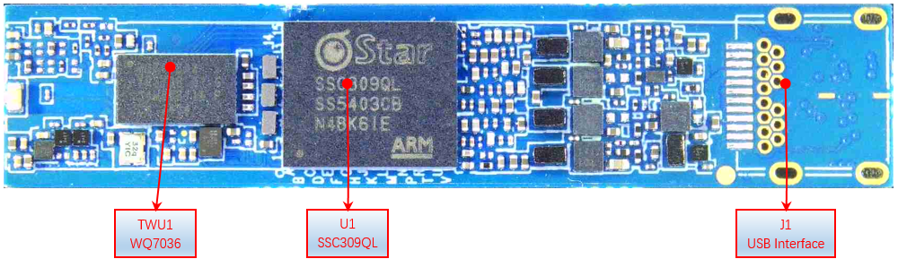
This guide will help you quickly get started with the COMAKE PI D2 development board and provide detailed information about this development board. The COMAKE PI D2 development board is based on the Sgs IPC main control chip SSC309QL and the WQ7036AX Bluetooth audio SoC, comprising a main board and an expansion board. For details, please refer to the subsequent sections.
1.1. System Introduction
- Power Input: 5V 1A, or 5V 2A (Type-C)
- Supports AI Glass/AOV and other functions
- The main chip is SSC309QL dual-core ARM Cortex-A32, with a maximum frequency of 1GHz;
- Onboard high-spec Bluetooth audio SoC chip WQ7036AX, suitable for advanced TWS noise-canceling headphones and other low-power products requiring complex audio processing and voice AI capabilities
- Supports WIFI6/BT/BLE5.4 dual-mode protocols and BLE Audio;
- VDD_CPU Voltage: default 0.9V, software settings can adjust voltage according to frequency;
- VDD_Core Voltage: default 0.9V, software settings can adjust voltage according to frequency;
- DRAM Voltage: LPDDR4X-1.8V, 1.1V, 0.6V;
- IO Voltage: 1.8V/3.3V
- Built-in 16bit 2Gbit LPDDR4X-3200Mbps
- Onboard 1.8V_EMMC capacity: 32GB;
- Supports 2.8-inch SPI Panel (maximum interface 720*360@30fps);
- Supports 4lane or 2lane (SR00) + 2lane (SR01) MIPI RX interfaces
- Equipped with 1 USB2.0 (can be configured as host or device via software);
- When the audio path uses TWS, it supports 2 (Channel) * 2 (PCS) DMIC. When using 309, it supports 1 (Channel) * 2 (PCS).;
- Supports digital audio output and analog audio output;
- Chip operating temperature range: -20°C ~ +70°C;
- Main Board Size:L(49mm)、W(10.2mm)、Thk(0.8mm)
- Expansion Board Size:L(97mm)、W(53.8mm)、Thk(1.6mm)
2. Interface Module Diagrams
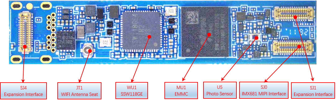
2.1. Main Board Interface Module Diagram
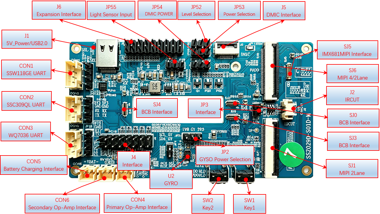
2.2. Expansion Board Interface Module Diagram
3. Detailed Description of Some Interface Modules
3.1 DC 5V 1A(J1)
J1 is a DC 5V Type-C power interface. When directly connecting 5V to the core board, the core board has a 5V to 4.2V LDO (because the TWS IC only supports power below 4.2V). The base board has this component mounted by default and can directly connect to 5V. Supports USB2.0.
3.2 Battery Interface (CON5)
TWS_Vbat battery interface, note that when using Type-C to charge the battery, NC expansion board R49 resistor is needed.
3.3 Photo/Video KEY (SW1)
Short press to take a photo, long press to record video.
3.4 Extended Button (SW2)
Extended function button. By default, it multiplexes the TWS Boot sel pin, and the button press will pull it high.
3.5 SSC309QL Debug Uart Interface (CON2)
SSC309QL Debug Uart, with a default baud rate of 115200, defaults to EMMC boot. CON2 can also switch to I2C mode, using the SigmaStar ISP Tool to upgrade uboot and read register information.
3.6 SSW118GE Debug Uart Interface (CON1)
SSW118GE WIFI Debug Uart, with a default baud rate of 115200.
3.7 WQ7036AX Debug Uart Interface (CON3)
WQ7036AX Debug Uart interface, with a default baud rate of 2M.
3.8 Primary Op-Amp Speaker Interface (CON4)


The primary op-amp is AW88082 digital op-amp, with I2S signals coming from TWS WQ7036AX. To verify, R92, R93 need to be confirmed.
Note
Note: If the core board audio uses 309QL, this op-amp will not work, and only the CON6 secondary op-amp will operate.
3.9 Secondary Op-Amp Interface (CON6)
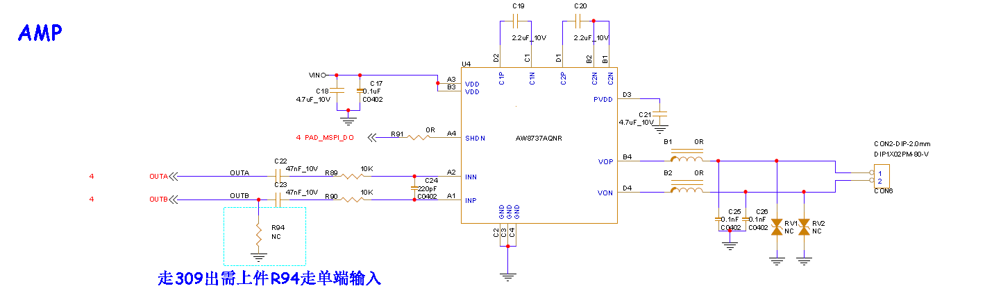
If the volume of the primary op-amp is insufficient, the secondary op-amp on the expansion board can be used. Ensure to disconnect the series resistors R92\R93 of the primary op-amp. The primary op-amp typically has high-frequency interference, so a low-pass filter circuit should be added to the secondary op-amp input to avoid background noise.
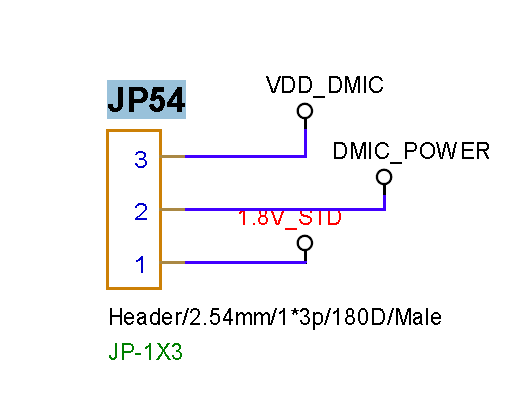
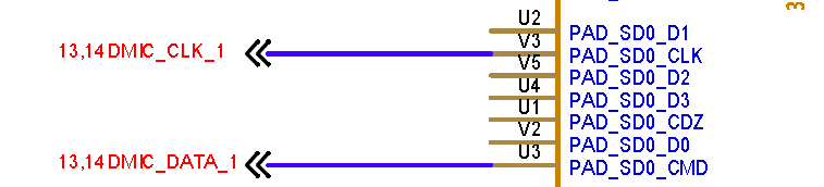
3.10 DMIC Interface (J5)
DMIC expansion interface. If using WQ7036AX, it supports up to 4 DMICs. If using 309, it supports up to 2 DMICs. Power can be selected via jumper to determine whether it is controlled by TWS.


3.11 GYSO Level Selection (JP2)
The expansion board GYSO supports free selection of IIC, and power supports switching between 3.3V/1.8V. The default IIC is in SSC309QL's I2CM0, and the default level is selected to be 1.8V. GYSO power is controlled by TWS WQ7036AX.

3.12 IRCUT Interface (J2)
IRCUT control interface, the default control IO needs to select to connect to JP3.


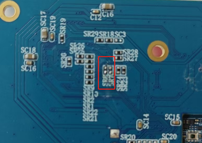
3.13 MIPI 4/2Lane Interface (SJ6)
Default supports MIPI 4Lane/2Lane; if connecting 4Lane for resolutions above 4K, remove the residual connections to the SJ5 seat.

| NC | SR1、SR2、SR7、SR8、SR21、SR22、SR23、SR24、SR25、SR26、SR27、SR28 |
|---|---|
For reference, see the effect after rework below:
3.14 IMX681 Module Interface (SJ5)
SJ5 is the IMX681 module interface, also compatible with the IMX471 module interface.

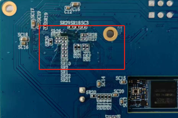
3.15 MIPI01 PAD2 2LANE Interface (SJ1)
SJ1 will be used when verifying MIPI 2Lane + 2Lane.

if connecing Sesnor using interface SJ1/SJ6 ,Requires NC components as follows to reduce signal residuals.
| NC | SR1、SR2、SR5、SR6、SR9、SR10、SR13、SR14、SR21、SR22、SR23、SR24、SR25、SR26、SR27、SR28 |
|---|---|
For reference, see the effect after rework below:
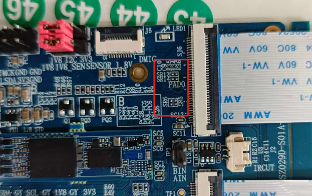
3.16 BCB Expansion Interface (SJ4, SJ0, SJ3)
SJ0 can connect to IMX681/471 module.

SJ3 and SJ4 are expansion IO interfaces, which can connect to different peripheral mainboards to verify different functions.


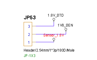
3.17 Sensor_1.8V Power Selection (JP53)
Select whether the 1.8V power for the sensor comes from the main board or the expansion board: 1.8V_STD is the expansion board power / Sensor_1.8V comes from the main board.
3.18 Expansion Interface (J4)

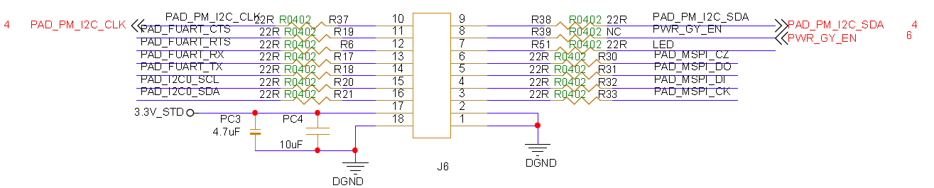
3.19 Expansion Interface (J6)
3.20 EMMC (MU1)
EMMC supports EMMC4.3 by default, with a maximum of 48MHz.
3.21 DMIC_POWER Selection (JP54)
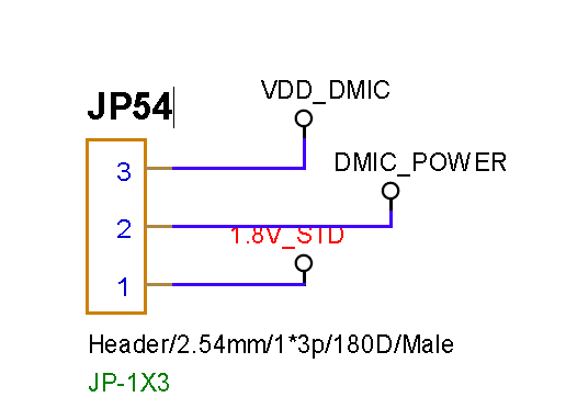
Select whether the DMIC power comes from VDD_DMIC (TWS) or from the base board's constant power 1.8V_STD.
3.22 Light Sensor Signal Input (JP55)
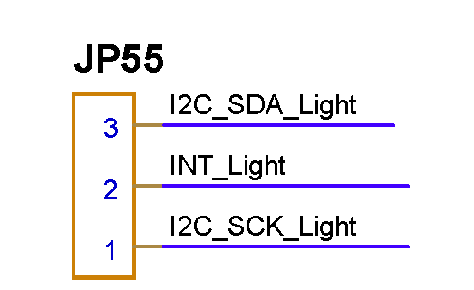
The base board supports OP3004 light sensor. JP55 needs to be connected with jumper wires to use other I2C for this module.
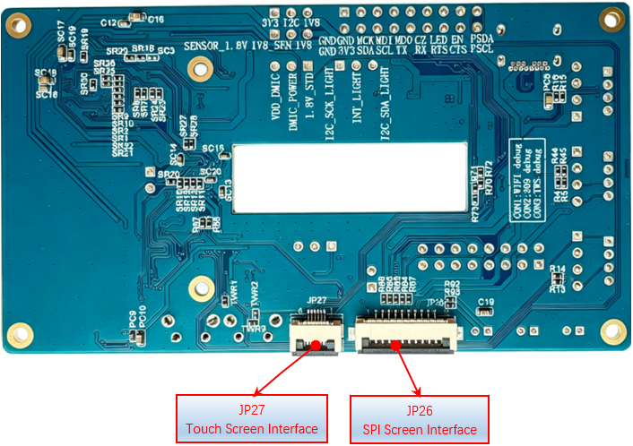
3.23 SPI Panel Interface (P26)
Note that the default selected SPI panel does not have an AE signal, which may cause jagged edges in motion pictures. If used for products, it is recommended to select a screen with AE signal.
4. Hardware Differences Between V1.0 and V2.0
4.1 Core Board
-
V1.0 hardware audio module can only use TWS, while V2.0 supports either TWS or SSC309QL, which requires hardware selection. See the schematic for details:
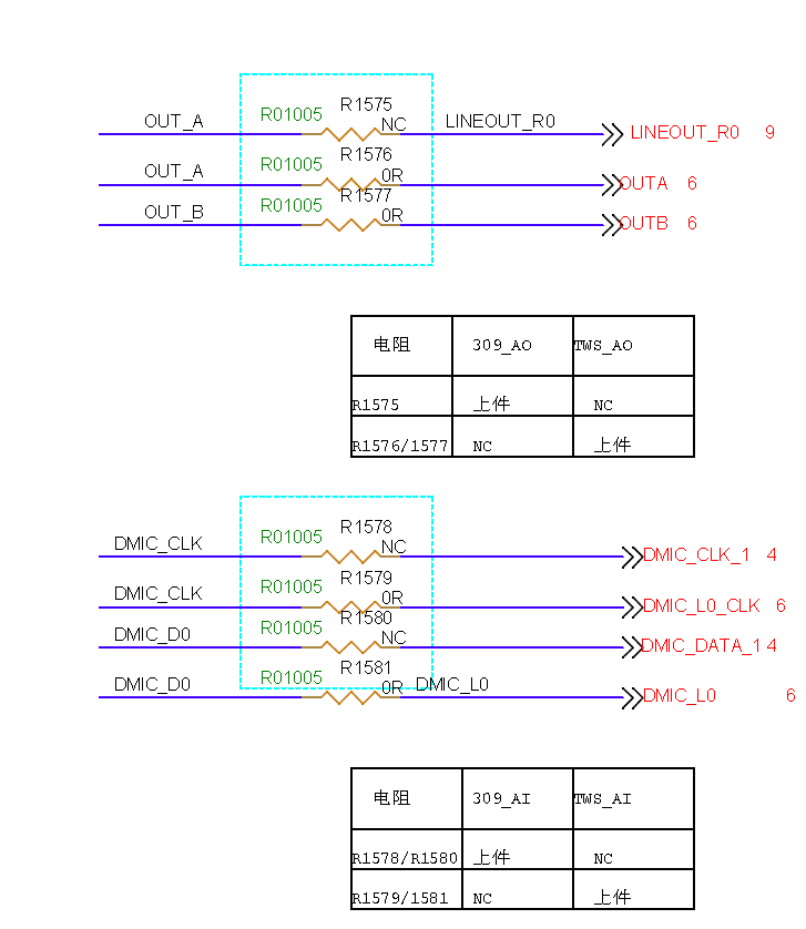
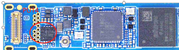
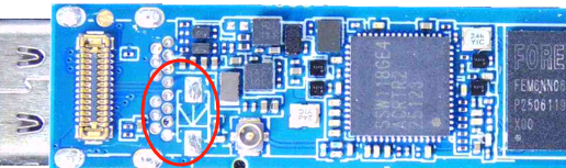
Physical details are as follows: the key indicator is R1575 NC, which means the default is TWS; conversely, if mounted, it uses 309.
Note
- If the core board audio uses 309QL, the AO Speaker can only connect to the CON6 secondary op-amp, and the primary op-amp will no longer work.
- If the core board audio uses 309QL, AI DMIC only supports 1 data line (connecting 2 DMICs). If using TWS, it can support 2 data lines (4 DMICs).
-
V2.0 adds a new 5V to 4.1V power conversion to improve power compatibility. V1.0 input relies on a diode to drop 0.7V.
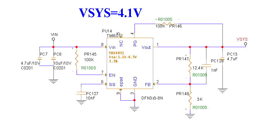
Therefore, the key distinguishing information between V1.0 and V2.0 hardware is whether there is PU14 next to the Type-C connector. V2.0 has it, while V1.0 has a diode instead of this LDO, as shown below:
-
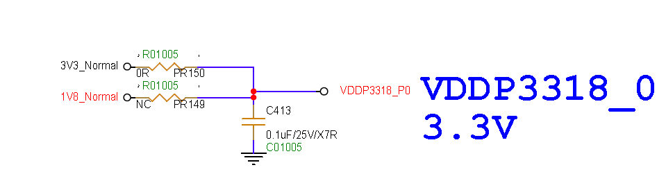
VDDP3318_P0 supports power switching, default is 3.3V
-
V2.0 corrects PAD_I2C2 wire sequence
4.2 Base Board
- V2.0 adds a new 5V to 4.1V power conversion to improve power compatibility. V1.0 input relies on a diode to drop 0.7V

-
V2.0 base board adds a Gyso module for convenient EIS debugging. V1.0 can only do this on the sensor adapter board
-
V2.0 adjusts the relative position of the core board and J4
-
V2.0 button SW2 is compatible with TWS_BOOT_SEL pin, facilitating button functions such as music playback
-
V2.0 serial port adds 2.54 pin headers for convenient debugging