SPI LCD Display User Guide
1. Overview
This guide describes how to configure the WL-28X0002 LCD display driver on the iford platform to enable display functionality.
1.1 Display Parameters
- Driver IC: ST7789V
- Screen Model: WL-28X0002-B-A20
- Resolution: 240 x 320 pixels
- Color Format: RGB565
- Interface: 4-wire SPI (56MHz)
1.2 Screen Interface Definition
The WL-28X0002-B-A20 screen connects to the Comake D2 development board through a 10-pin FPC interface. The interface pin definitions are as follows:
| Pin No. | Signal Name | Function Description | Connect to Dev Board |
|---|---|---|---|
| 1 | GND | Ground, provides reference potential | GND |
| 2 | RS / DCX | Register Select (Data/Command Select) | PAD_MSPI_CK |
| 3 | /CS | Chip Select (active low) | PAD_SPI0_CZ |
| 4 | SCL / SCLK | Serial Clock Input | PAD_SPI0_CK |
| 5 | SDA / MOSI | Serial Data Input | PAD_SPI0_DI |
| 6 | RESET | Reset Signal (active low) | PAD_MSPI_CK |
| 7 | VCC | Logic Power Supply (1.8V or 3.3V) | 3.3V_STD |
| 8 | GND | Ground | GND |
| 9 | A | LED Backlight Anode (Positive) | 3.3V_STD |
| 10 | K | LED Backlight Cathode (Negative) | 3.3V_STD |
Signal Description:
- RS/DCX: High level for display data transfer, low level for command transfer
- /CS: Low level enables screen communication, high level screen ignores input signals
- SCL/SCLK: SPI clock signal for synchronizing data transfer
- SDA/MOSI: SPI master output data line
- RESET: Low level resets screen registers to default state
- VCC: Powers screen logic circuitry (voltage may be 1.8V or 3.3V depending on screen model)
- A/K: LED backlight power pins for controlling screen backlight
2. Driver Configuration
2.1 Kernel Configuration
The FBTFT driver is located at kernel/drivers/staging/fbtft/. To enable ST7789V LCD support, add the following configuration to the kernel defconfig (e.g., arch/arm/configs/iford_ssc029d_s01a_d2_full_defconfig):
# FBTFT framework (built into kernel)
CONFIG_FB_TFT=y

# ST7789V driver (built into kernel)
CONFIG_FB_TFT_ST7789V=y
2.2 Device Tree Configuration
2.2.1 ST7789V Device Node
Add to arch/arm/boot/dts/iford.dtsi:
#if IS_ENABLED(CONFIG_SSTAR_QSPI)
        qspi: spi@0x1f201A00 {
            compatible = "sstar,qspi";
            reg = <0x1F201A00 0x200>, <0x1F201C00 0x200>;
            clocks = <&CLK_fsp_qspi>, <&CLK_spi_nonpm>, <&CLK_spi_synth_pll>;
            qspi-group = <3>;
            #address-cells = <1>;
            #size-cells = <0>;
            dma-write-en;
            #dma-read-en;
            width_ctrl = <0>;
            cs-mode = <2>;
            cs-num = <1>;
            // cs-ext = <PAD_FUART_TX>;
            status = "ok";
            spi-cpol;

            wl28x0002@0 {
                compatible = "sitronix,st7789v";
                reg = <0>;
                status = "ok";
                spi-max-frequency = <54000000>;
                rotate = <0>;
                fps = <20>;
                buswidth = <8>;
                spi-tx-bus-width = <1>;
                spi-rx-bus-width = <1>;
                dc-gpios = <&gpio PAD_MSPI_CK 0>;
                reset-gpios = <&gpio PAD_MSPI_DI 1>;
                txbuflen = <4096>;
                debug = <1>;
            };

        };
#endif
2.3 Pin Configuration
When using QSPI, pins are enabled by default and no padmux configuration is required.
3. System Architecture
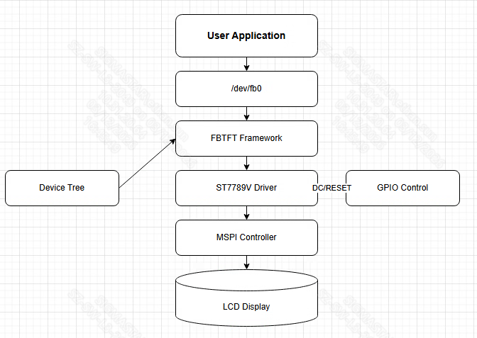
Figure: SPI LCD system architecture showing data flow and connection relationship from user application to LCD hardware
4. Hardware Connection Example
The following example shows the actual connection between the WL-28X0002-B-A20 screen and the Comake D2 development board:
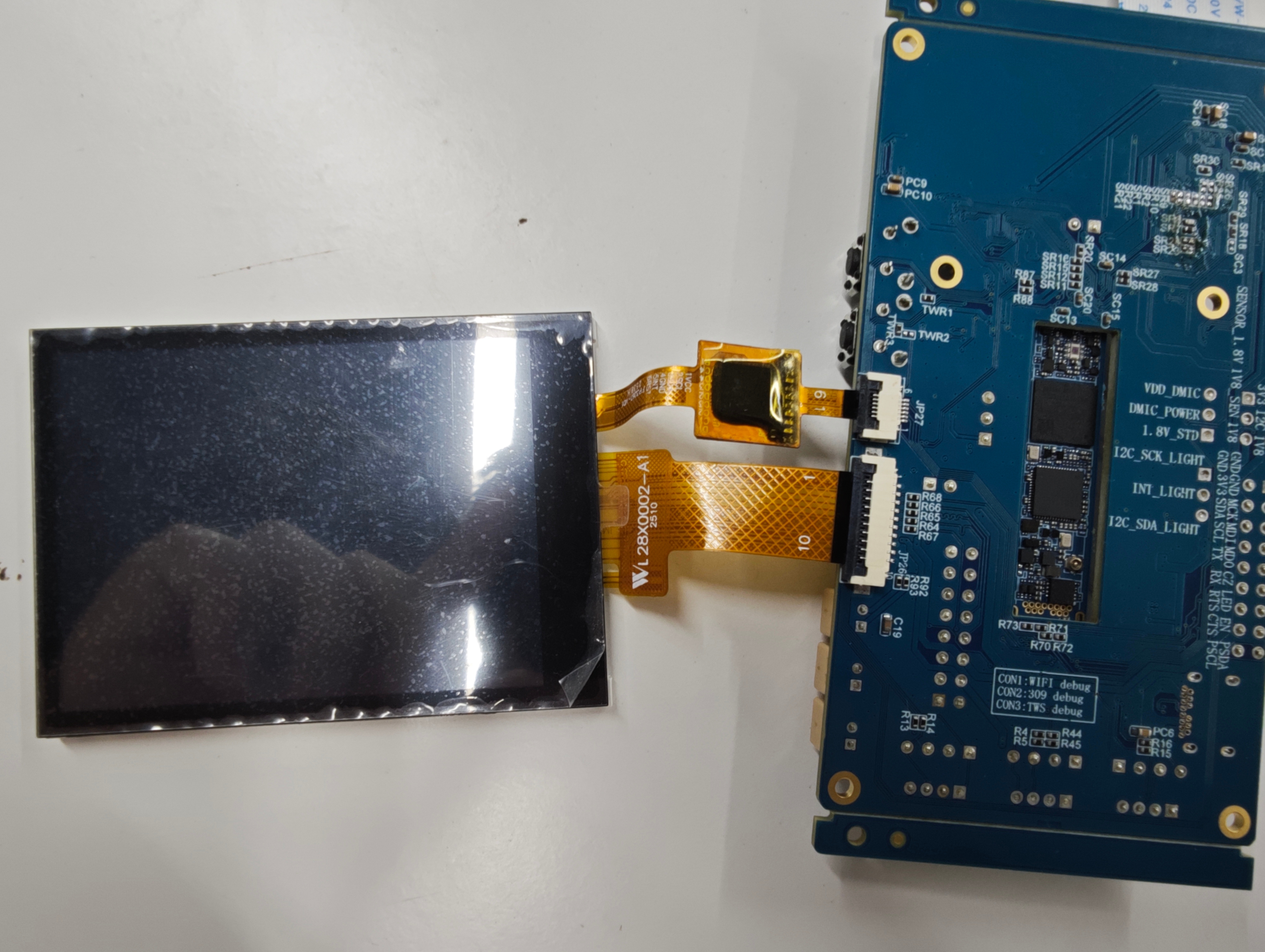
Figure: Hardware connection example of WL-28X0002-B-A20 screen to SSC035A-S01A-S development board
The following diagram shows the 10-pin SPI interface pinout definition of the WL-28X0002-B-A20 screen:
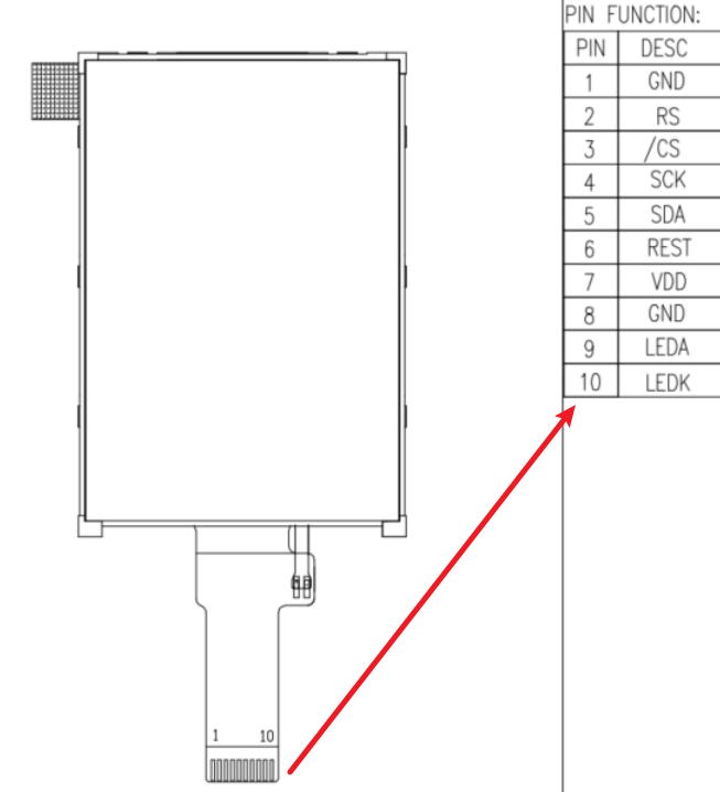
Figure: WL-28X0002-B-A20 screen 10-pin SPI interface pinout diagram
Connection Points:
- The screen connects to the development board through a 10-pin FPC interface
- SPI signals (SCL, SDA, /CS) are connected as shown in the example
- Control signals (RS, RESET) are controlled through GPIO pins
- Power and backlight signals are supplied through corresponding power networks
5. Initialization Sequence
The driver initializes ST7789V using the following sequence (from fb_st7789v.c:init_display()):
- Hardware reset
- Initialize tearing effect line (if configured)
- Exit sleep mode (0x11) - 120ms delay
- Set pixel format to RGB565 (0x3A, 0x05)
-
Set porch control (0xB2):
- HSD20_IPS panel: 0x05, 0x05, 0x00, 0x33, 0x33
- Other panels: 0x08, 0x08, 0x00, 0x22, 0x22
-
Gate control (0xB7):
- HSD20_IPS panel: 0x75 (VGH=13.26V, VGL=-10.43V)
- Other panels: 0x35
-
Enable VDV and VRH command (0xC2): 0x01, 0xFF
-
Set VRH (0xC3):
- HSD20_IPS panel: 0x13
- Other panels: 0x0B
-
Set VDV (0xC4): 0x20 (VDV=0V)
-
Set VCOM (0xBB):
- HSD20_IPS panel: 0x22 (VCOM=0.9V)
- Other panels: 0x20
-
Set VCOM offset (0xC5): 0x20 (VCOM offset=0V)
-
Power control (0xD0): 0xA4, 0xA1
- AVDD = 6.8V
- AVCL = -4.8V
- VDS = 2.3V
-
TE line output (if configured): 0x35, 0x00 (turn off)
- Turn on display (0x29)
- Enable display inversion (0x21) for HSD20_IPS panels
5.1 Key Commands
| Command | Hex | Description |
|---|---|---|
| 0x11 | SLPOUT | Exit sleep mode |
| 0x29 | DISPON | Turn on display |
| 0x21 | INVON | Enable display inversion |
| 0x2C | RAMWR | Memory write |
| 0x35 | TEEON | Tearing effect line on |
| 0x3A | COLMOD | Pixel format setting (16-bit RGB565) |
| 0x36 | MADCTL | Memory access control (set in set_var()) |
| 0xB2 | PORCTRL | Porch setting |
| 0xB7 | GCTRL | Gate control |
| 0xBB | VCOMS | VCOM setting |
| 0xC2 | VDVVRHEN | VDV and VRH command enable |
| 0xC3 | VRHS | VRH set |
| 0xC4 | VDVS | VDV set |
| 0xC5 | VCMOFSET | VCOM offset set |
| 0xD0 | PWCTRL1 | Power control 1 |
| 0xE0 | PVGAMCTRL | Positive voltage gamma control |
| 0xE1 | NVGAMCTRL | Negative voltage gamma control |
6. Compilation and Loading
6.1 Compile Kernel
# Navigate to kernel directory
cd kernel

# Select defconfig
make iford_ssc029d_s01a_d2_full_defconfig

# Compile kernel
make -j8
6.2 Load Driver Module
After being built into the kernel, it loads automatically on startup
6.3 Verify Driver Loading
# Check frame buffer device
ls -l /dev/fb*

# View driver info
cat /sys/class/graphics/fb0/name
cat /sys/class/graphics/fb0/modes
7. Test Display
The sample code includes a framebuffer test program for ST7789V LCD:
Source code: sdk/verify/sample_code/source/iford/disp/spi_demo/spi_demo.c
Compile:
cd sdk/verify/sample_code/
make clean && make source/iford/disp/spi_demo
The generated target is in the ./out path
Run on target device:
# Run test program
./prog_disp_spi_demo
The test program will perform the following operations:
Display red/green/blue color bar patterns on the SPI screen in a loop
After the program runs normally, the SPI screen will display color bar patterns in a loop:
-
The screen is divided into three equal parts, displaying different colors
-
buffer 0: left red, middle green, right blue
-
buffer 1: left blue, middle red, right green
-
Switch between the two patterns every 3 seconds
8. Debug Information
8.1 Check Kernel Logs
# View driver initialization
dmesg | grep -i st7789v

# Check FBTFT logs
dmesg | grep -i fbtft
8.2 Common Issues
Display not working:
- Check device tree configuration
- Verify DC and RESET pin configuration
- Confirm SPI clock frequency (try 16MHz)
- Check kernel error logs
Color abnormal:
- Confirm BGR mode configuration
- Check pixel format setting