Adc_DebugSop
REVISION HISTORY
| Revision No. | Description |
Date |
|---|---|---|
| 1.0 | 2024/03/07 |
1. Debug Flow Chart
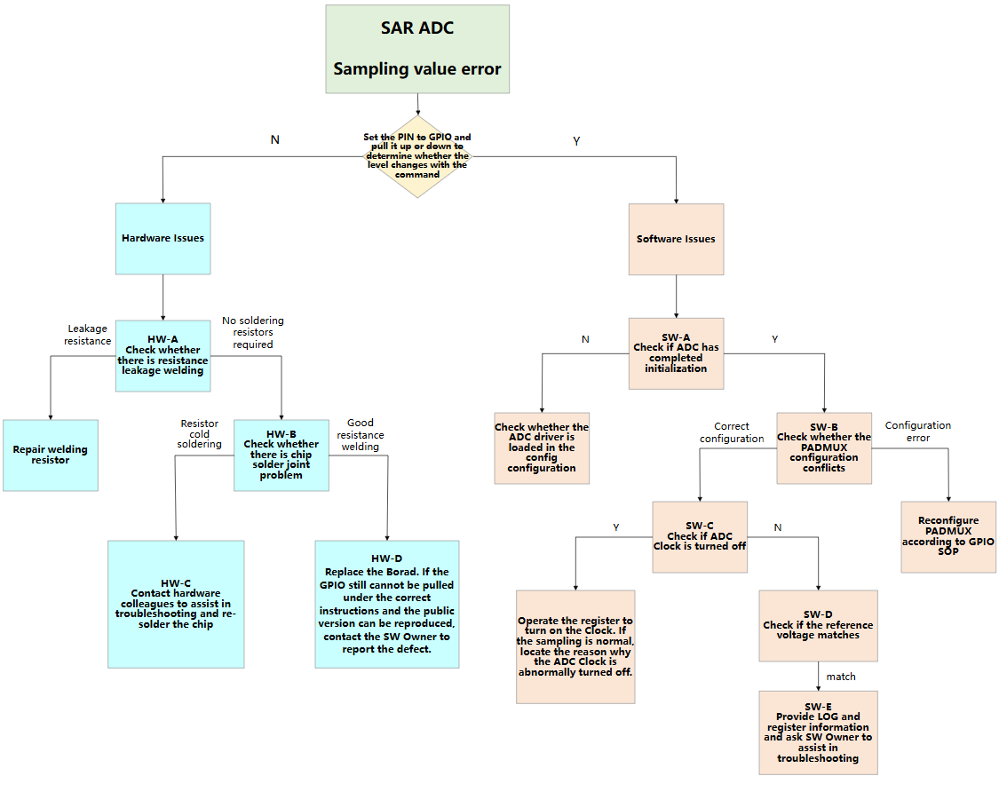
2. Debug Process Description
2.1 Hardware Issues
When SAR ADC sampling errors are detected, registers can be configured to set the corresponding PIN to GPIO and pull it high/low (Note: For certain PINs, GPIO function priority is not the highest. In such cases, higher-priority configurations must be cleared first). Operation method:
riu_w 0x14 0x11 0x00  // Set to GPIO MODE
riu_w 0x14 0x12 0xff  // Set to high level
riu_w 0x14 0x12 0x00  // Set to low level
If the actual output level does not change, it can be determined as a hardware issue. Perform troubleshooting in the following sequence:
2.1.1 HW-A Check Resistors
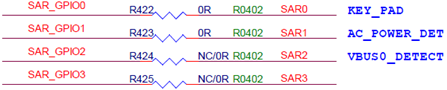
Verify whether resistors are missing on the corresponding PIN in the schematic. As shown in the figure below, resistors R424 and R425 must be populated with 0R resistors.
2.1.2 HW-B Check Soldering Status
If GPIO can be pulled high/low after replacing the board, the chip may have poor soldering. Rework is required.
2.1.3 HW-C Request Assistance
Contact hardware colleagues to assist with troubleshooting and chip rework.
2.1.4 HW-D Defect Reporting
If GPIO still cannot be pulled high/low after replacing the board, contact the SW Owner to report the defect.
2.2 Software Issues
When determined as a software issue, perform troubleshooting in the following sequence:
2.2.1 SW-A Check ADC Initialization Status
Verify whether ADC initialization is completed through Bank 0x14 configuration. Primarily check whether the value of 0x0 is 0xA20, and whether 0x40~0x47 contain values:
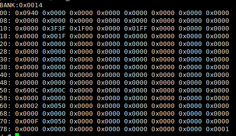
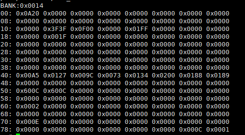
If initialization is not completed, sampling cannot be performed. Verify whether the SAR ADC driver is loaded in the config configuration.
Linux config:
Device Drivers --->
[*] Sstar SoC platform drivers --->

    <*> Sstar ADCLP driver
Linux DTS:
adclp0: adclp0@1f002800 {    // Select channel 0
    compatible = "sstar,adclp";
    ......
    status = "ok";  // Ok: Initialize adc
};
Rtos config:
BSP Driver Options --->

    <*> Support SARADC driver
Rtos Sysdesc:
<adclp0>     // Select channel 0
    [reg_u32] 0x1F002800;
    ......
    [status_u8] 1; // 1: Initialize adc
2.2.2 SW-B Check PADMUX
After ADC initialization, if voltage values still cannot be obtained correctly, check whether PADMUX conflicts exist. Refer to the PADMUX conflict checking section in Gpio_DebugSop. Generally, ADC pins cannot perform sampling after being set to GPIO MODE.
2.2.3 SW-C Check Clock Source
Check the following registers to verify whether the ADC clock source is disabled. Taking iford as an example:
0xE 0x22 BIT5
If BIT5 = 0, the ADC clock source is enabled. If BIT5 = 1, it indicates the ADC clock source is abnormally disabled. Contact the SW Owner for debugging.
2.2.4 SW-D Check Reference Voltage
Check the following registers to verify the reference voltage range of each ADC channel. Taking iford as an example (register positions are consistent for other chips):
0x14 0x19 BIT0 corresponds to channel 0, BIT1 corresponds to channel 1, and so on
When the BIT value is 1, the reference voltage for that channel is 1.8V. When the BIT value is 0, the reference voltage for that channel is 1.0V. (For some chips, BIT 1/0 corresponds to reference voltages of 3.3V/2.0V). Confirm whether mismatched reference voltage was used during voltage calculation.
2.2.5 SW-E Request Assistance
If all previous steps SW-A, SW-B, SW-C, and SW-D are verified OK, please provide ADC-related LOG and ADC BANK (0x14) information, and contact the SW Owner for debugging.