Screen Parameter Usage Guide
REVISION HISTORY
| Revision No. | Description |
Date |
|---|---|---|
| 1.0 | 02/22/2024 | |
| 1.1 | 05/12/2025 | |
| 1.2 | 11/06/2025 | |
| 1.3 | 04/30/2026 | |
| 1.4 | 07/22/2026 |
1. Basic Introduction
1.1 Overview
As the name suggests, screen parameters refer to the parameter configurations used by the screen. This document mainly explains the configuration of point screen, the meaning of screen parameters, and how to set the correct screen parameters.
1.2. Keyword Description
-
TTL/BT656/SRGB/MIPI-DSI
TTL: Transistor-Transistor Logic, The interface signal is a digital signal that transmits parallel RGB data.
BT656: The interface signal is a digital signal that transmits YUV data.
SRGB: Series RGB, The interface signal is a digital signal that transmits serial RGB data.
MIPI-DSI: Mobile Industry Processor Interface-Display Serial Interface, The interface signal is transmitted as a differential signal, transmitting RGB data, with high-speed HS and low-speed LP modes.
2. Screen Parameter Configuration File
2.1 Screen Parameter Configuration File Path
project\board\$(chip)\screen_param\config_disp.json
project\board\$(chip)\$(boardname)\config\config_board.json
2.2 Screen Parameter Configuration File Composition
During the image build process, the files config_disp.json, config_board.json, and config_fb.json are merged into a single config.json file, which is then copied to its corresponding partition.
During the system startup process, the screen parameter configuration file will be parsed, and then different screen parameters will be saved in the system for use by the display module. The display module will obtain the required screen parameters from the system according to the parameter settings of the user calling the API.
2.2.1 config_disp.json
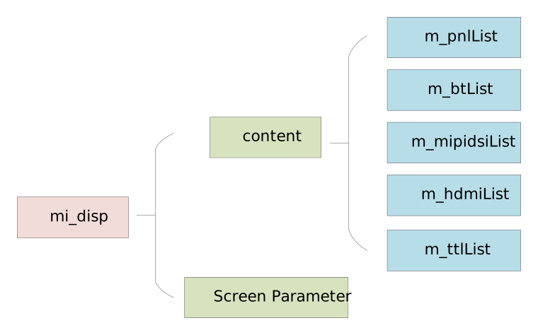
The config_disp.json file describes the supported display parameters. Its structure is illustrated in the following diagram. The root node is mi_disp, which contains two child nodes: content and screen_parameter.
The content node is a collection of screen parameter name lists, including four sub-nodes: m_pnlList, m_btList, m_mipidsiList and m_hdmiList.
-
m_pnlList
"m_pnlList": [
    "SAT070AT50H18BH",
    "RM68200_LX50HDH40145",
    ......
    "DUAL_LVDS_SG2151B04"
]
m_pnlList lists various user-defined screen parameter names. This denotes that m_ePanelTiming=E_MI_DISP_OUTPUT_USER(52).
-
m_btList
"m_btList": [
    "BT656OUT_576P_50",
    "BT656OUT_480P_60",
    "BT656OUT_1080P_25",
    "BT656OUT_1080P_30",
    "BT656OUT_720P_25",
    "BT656OUT_720P_30",
    "BT656OUT_720P_50",
    "BT656OUT_720P_60",
    "BT601OUT_576P_50",
    "BT601OUT_480P_60",
    "BT601OUT_1080P_25",
    "BT601OUT_1080P_30",
    "BT601OUT_720P_25",
    "BT601OUT_720P_30",
    "BT601OUT_720P_50",
    "BT601OUT_720P_60",
    "BT1120OUT_576P_50",
    "BT1120OUT_480P_60",
    "BT1120OUT_1080P_25",
    "BT1120OUT_1080P_30",
    "BT1120OUT_1080P_50",
    "BT1120OUT_1080P_60",
    "BT1120OUT_720P_25",
    "BT1120OUT_720P_30",
    "BT1120OUT_720P_50",
    "BT1120OUT_720P_60"
]
m_btList lists the screen parameter names of BT601/BT656/BT1120 with multiple standard resolutions
-
m_mipidsiList
"m_mipidsiList": [
    "MIPIDSI_480P_60",
    "MIPIDSI_576P_50",
    "MIPIDSI_720P_30",
    "MIPIDSI_720P_50",
    "MIPIDSI_720P_60",
    "MIPIDSI_1080P_25",
    "MIPIDSI_1080P_30",
    "MIPIDSI_1080P_50",
    "MIPIDSI_1080P_60",
    "MIPIDSI_4KP_30"
]
m_mipidsiList lists the screen parameter names of mipidsi with multiple standard resolutions.
-
m_hdmiList
"m_hdmiList": [
    "DACOUT_800x600P_60",
    "DACOUT_720P_24",
    "DACOUT_720P_25",
    "DACOUT_720P_2997",
    "DACOUT_720P_30",
    "DACOUT_720P_50",
    "DACOUT_720P_5994",
    "DACOUT_720P_60",
    ......
    "DACOUT_4KP_30"
]
m_hdmiList lists the screen parameter names of hdmi and vga with multiple standard resolutions.
-
Screen Parameter
The screen parameters are composed of section and variable name:
"SAT070AT50H18BH": {
    "m_wPanelDispPath":       0,
    "m_pPanelName": "SAT070AT50H18BH",
    "m_ePanelTiming":         52,
    "m_ePanelIntfType":       9,
    "m_wPanelHSyncWidth":     48,
    "m_wPanelHSyncBackPorch": 46,
    "m_wPanelVSyncWidth":     4,
    "m_wPanelVBackPorch":     23,
    "m_wPanelHStart":         98,
    "m_wPanelVStart":         27,
    "m_wPanelWidth":          1024,
    "m_wPanelHeight":         600,
    "m_wPanelHTotal":         1344,
    "m_wPanelVTotal":         635,
    "m_wPanelDCLK":           51000000,
    "m_ucPanelSwapChnR":      3,
    "m_ucPanelSwapChnG":      2,
    "m_ucPanelSwapChnB":      1,
    "m_ucPanelSwapRgbML":     0
},
The section refers to the screen parameter name in the figure, EX: "SAT070AT50H18BH".
The variable name refers to the field on the left side of ":", and the right side is the value assigned to the variable name.
The section is unique and do not allow duplicate names. Furthermore, the section name must match the value of m_pPanelName to ensure the correct retrieval of the screen parameters.
2.2.2 config_board.json
The config_board.json file describes hardware-related information and default configurations for the board. Its structure is illustrated in the following diagram. The root node is board, which contains four child nodes: bootlog, dev_property, pq, and power_sequence.
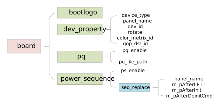
For a description of the bootlogo node, please refer to: bootlogo
-
dev_property
Parameters Description device_type Screen Type. This parameter is used by bootlogo.
TTL/BT656/SRGB/MCU/MCU_NOFLM/MIPIDSIpanel_name Panel Parameter Name dev_id device id rotate Rotation Parameter. This parameter is used by bootlogo.
0:0°
90:90°
180:180°
270:270°color_metrix_id csc metrix id gop_dst_id This parameter is currently disabled. This node describes the default configuration information shared by mi_disp and bootlogo. The default screen parameters are retrieved by the panel_name.
-
pq
Parameters Description pq_enable PQ function enable pq_file_path PQ.bin file path -
power_sequence
Parameters Description ps_enable power sequence function enable panel_name panel parameter name to be replaced m_pAfterLP11 m_pAfterLp11 content to be replaced m_pAfterInit m_pAfterInit content to be replaced m_pAfterDeinitCmd m_pAfterDeinitCmd content to be replaced To address specific power sequencing requirements for MIPI DSI screens, a dedicated panel parameter has been designed for user-defined configuration. For specific implementation details, refer to the MIPIDSI interface specific parameters section of this document.
Since different package types may involve different hardware designs, the power sequencing configuration must be adjusted accordingly. In this case, you can configure the power_sequence node in config_board.json by setting ps_enable to ON. During the image build process where config.json is generated, the screen parameter content corresponding to the power_sequence node will be replaced.
2.3 Screen Parameter Configuration File Loading Mechanism
During system startup, the screen parameter configuration file is searched in a fixed order. The system tries the following paths in turn, and the first path that can be successfully opened and parsed as valid JSON is adopted (refer to MI_COMMON_CJSON_InitCustomerCjson in sdk/impl/common/mi_common_cjson.c):
| Order | Path |
|---|---|
| 1 | /misc/config.json |
| 2 | /config/config.json |
Behavior when the misc partition is mounted but contains no file: The loading logic only cares whether the configuration file can be opened, and is independent of whether the misc partition is mounted. When the misc partition is mounted but there is no config.json in it, the first path /misc/config.json fails to open and the system automatically falls through to the second path /config/config.json, and so on.
Dynamically loading an arbitrary path at runtime: In addition to the static lookup at startup, the configuration file path can be dynamically specified at runtime through the proc node:
The written path has no whitelist restriction; as long as the file at that path exists and is valid JSON, it can be loaded (for example, paths like /customer/config.json that are not in the startup lookup list). This operation refreshes the configuration of the first node of the internal linked list in place. The DISP module picks up the new configuration on its next initialization or reconfiguration (refer to _MI_DISP_IMPL_ConfigInit in sdk/impl/disp/mi_disp_impl.c), thereby taking effect dynamically.
3. New Screen Parameters and the Retrieval Process
3.1 New Screen Parameters
-
The section name of the newly added screen parameter definition is not allowed to be the same as the existing section name
-
The name of the newly added screen parameter node can be appended to m_pnlList.
-
The following shows an example of adding new screen parameters in the screen parameter node:
"mi_disp": {
    "content": {
        "m_pnlList": [
            "RM68200_LX50HDH40145",
            "SAT070AT50H18BH"
        ],
        ......
    },
    "SAT070AT50H18BH": {
        "m_wPanelDispPath":       0,
        "m_pPanelName": "SAT070AT50H18BH",
        "m_ePanelTiming":         52,
        "m_ePanelIntfType":       9,
        "m_wPanelHSyncWidth":     48,
        "m_wPanelHSyncBackPorch": 46,
        "m_wPanelVSyncWidth":     4,
        "m_wPanelVBackPorch":     23,
        "m_wPanelHStart":         98,
        "m_wPanelVStart":         27,
        "m_wPanelWidth":          1024,
        "m_wPanelHeight":         600,
        "m_wPanelHTotal":         1344,
        "m_wPanelVTotal":         635,
        "m_wPanelDCLK":           51000000,
        "m_bPanelInvDCLK":        0,
        "m_bPanelInvDE":          0,
        "m_bPanelInvHSync":       0,
        "m_bPanelInvVSync":       0,
        "m_ucPanelSwapChnR":      3,
        "m_ucPanelSwapChnG":      2,
        "m_ucPanelSwapChnB":      1,
        "m_ucPanelSwapRgbML":     0
    },
    ......
}
3.2 Screen Parameter Retrieval Process
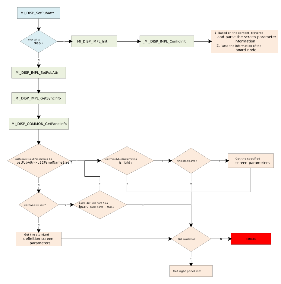
Currently, there are three methods to retrieve specific screen parameters: obtaining via user interface parameter passing, acquiring standard-defined parameters by specifying eIntfType and eIntfSync, and retrieving default custom parameters from the board node.
The highest priority is given to the method where the user passes parameters by calling the MI_DISP_SetPubAttr interface. It first searches for the specified screen parameter based on the user-provided pu8PanelName.
If the pu8PanelName passed to MI_DISP_SetPubAttr is NULL or u32PanelNameSize is 0, the system then checks whether the currently passed eIntfSync is E_MI_DISP_OUTPUT_USER.
If it is user, the system looks for the default screen parameter specified in the board node. If it is not user, the standard-defined screen parameter is located based on eIntfType and eIntfSync.
The parsing/retrieval flow is as follows:
4. Screen Parameter Description
4.1 Public Parameters
| Parameters | Description |
|---|---|
| m_pPanelName | panel name |
| m_ePanelTiming | Output resolution, 52 means user-defined |
| m_ePanelIntfType | Interface type VGA:2 BT656:3 BT1120:4 HDMI:5 TTL:9 MIPIDSI:10 SRGB:12 MCU:13 MCU_NOFLM:14 BT601:15 BT1120-DDR:16 LVDS:17 LVDS1:18 DUAL-LVDS:19 MIPIDSI1:20 |
| m_wPanelHSyncWidth | Line synchronization signal pulse width |
| m_wPanelHSyncBackPorch | Horizontal synchronization signal back porch |
| m_wPanelVSyncWidth | Vertical synchronization signal pulse width |
| m_wPanelVBackPorch | Vertical synchronization signal back porch |
| m_wPanelHStart | m_wPanelHSyncWidth+m_wPanelHSyncBackPorch |
| m_wPanelVStart | m_wPanelVSyncWidth+m_wPanelVBackPorch |
| m_wPanelWidth | Number of effective pixels in horizontal direction |
| m_wPanelHeight | Number of effective pixels in vertical direction |
| m_wPanelHTotal | m_wPanelWidth+m_wPanelHSyncWidth+m_wPanelHSyncBackPorch+HsyncFrontPorch |
| m_wPanelVTotal | m_wPanelHeight+m_wPanelVSyncWidth+m_wPanelVBackPorch+VsyncFrontPorch |
| m_wPanelDCLK | pixel clk: m_wPanelHTotal * m_wPanelVTotal * fps |
| m_bPanelInvDCLK | pixel clk polarity inversion |
| m_bPanelInvHSync | Hsync polarity inversion |
| m_bPanelInvVSync | Vsync polarity inversion |
| m_wSpreadSpectrumFreq | Clock spread spectrum frequency modulation (for details, see spreadSpectrumFreqCalculation) |
| m_wSpreadSpectrumRatio | Clock spread spectrum ratio modulation (for details, see spreadSpectrumFreqCalculation) |
| m_ucPanelSwapChnR | Swap channel R default = 0(Maintain the original connection of the physical circuit, that is, the R channel uses the corresponding signal source in the hardware design) 1: select R(Forcefully cover the channel signal source and replace the R-channel data with the R-channel signal output by the main control) 2: select G 3: select B |
| m_ucPanelSwapChnG | Swap channel G default = 0 1: select R 2: select G 3: select B |
| m_ucPanelSwapChnB | Swap channel B default = 0 1: select R 2: select G 3: select B |
| m_ucPanelSwapRgbML | Swap RGB MSB/LSB 0: disable M/L swap 1: enable M/L swap |
| m_ePanelRgbDataType | RGB data type or LCD data bus 0:E_MI_DISP_MHALPNL_RGB_DTYPE_RGB888, 1:E_MI_DISP_MHALPNL_RGB_DTYPE_RGB666, 2:E_MI_DISP_MHALPNL_RGB_DTYPE_RGB565, 3:E_MI_DISP_MHALPNL_RGB_DTYPE_RGB444, 4:E_MI_DISP_MHALPNL_RGB_DTYPE_RGB333, 5:E_MI_DISP_MHALPNL_RGB_DTYPE_RGB332, 6:E_MI_DISP_MHALPNL_RGB_DTYPE_BGR888, 7:E_MI_DISP_MHALPNL_RGB_DTYPE_BGR666, 8:E_MI_DISP_MHALPNL_RGB_DTYPE_BGR565, 9:E_MI_DISP_MHALPNL_RGB_DTYPE_BGR444, 10:E_MI_DISP_MHALPNL_RGB_DTYPE_BGR333, 11:E_MI_DISP_MHALPNL_RGB_DTYPE_BGR332, 12:E_MI_DISP_MHALPNL_RGB_DTYPE_YUV422_UY0VY1, 13:E_MI_DISP_MHALPNL_RGB_DTYPE_YUV422_VY0UY1, 14:E_MI_DISP_MHALPNL_RGB_DTYPE_YUV422_UY1VY0, 15:E_MI_DISP_MHALPNL_RGB_DTYPE_YUV422_VY1UY0, 16:E_MI_DISP_MHALPNL_RGB_DTYPE_YUV422_Y0UY1V, 17:E_MI_DISP_MHALPNL_RGB_DTYPE_YUV422_Y0VY1U, 18:E_MI_DISP_MHALPNL_RGB_DTYPE_YUV422_Y1UY0V, 19:E_MI_DISP_MHALPNL_RGB_DTYPE_YUV422_Y1VY0U |
| m_ePanelRgbDeltaOddMode | delta mode Odd Field Data Arrangement 0: RGB 1: RBG 2: GRB 3: GBR 4: BRG 5: BGR |
| m_ePanelRgbDeltaEvenMode | delta mode Arrangement of Even Field Data 0: RGB 1: RBG 2: GRB 3: GBR 4: BRG 5: BGR |
| m_ePanelRgbDataSwap | RGB data swap for all data 0: disable 1: enable |
| m_wPadDrvngLvl | Pin drive strength adjustment. Set the drive strength level for all pins of the interface. There are 4 levels in total. 0: 4mA 1: 8mA 2: 12mA 3: 16mA |
Note: 12~19 of m_ePanelRgbDataType are optional for BT interface.
Schematic diagram of normal timing for m_bPanelInvDCLK, m_bPanelInvHSync and m_bPanelInvVSync:

Schematic diagram of enabling polarity reversal timing for m_bPanelInvDCLK, m_bPanelInvHSync and m_bPanelInvVSync:

4.2 BT Interface Specific Parameters
The panel defaults to P mode for progressive scanning. If it is BT601/BT656/BT1120, you can also choose I mode for interlaced scanning. The following parameters need to be configured. The following figure takes BIT656 525 lane as an example.
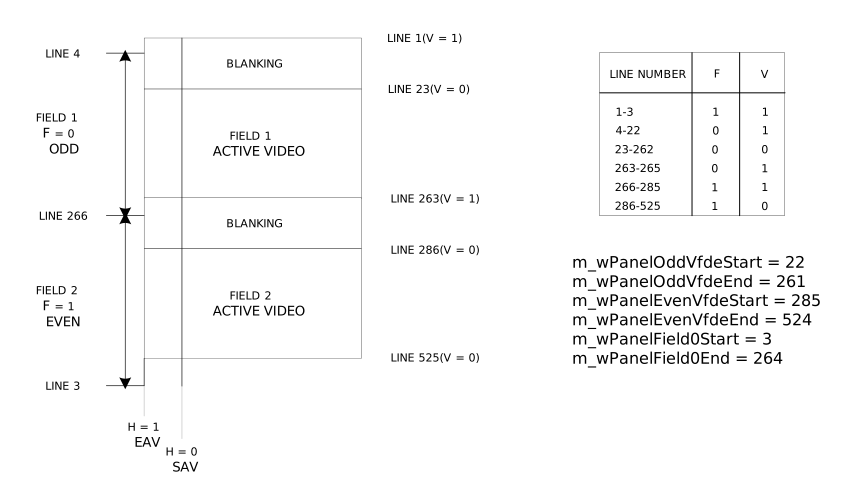
| Parameters | Description |
|---|---|
| m_ePanelScanMode | scan mode 0:default 1:old P mode 2:new P mode 3:I mode |
| m_wPanelOddVfdeStart | vertical active start point for I mode odd field |
| m_wPanelOddVfdeEnd | vertical active end point for I mode odd field |
| m_wPanelEvenVfdeStart | vertical active start point for I mode even field |
| m_wPanelEvenVfdeEnd | vertical active end point for I mode even field |
| m_wPanelField0Start | field0 start point for I mode |
| m_wPanelField0End | field0 end point for I mode |
Note: The difference between old P mode and new P mode is the hardware pathway, and the data output to the screen is the same.
4.3 MIPIDSI interface specific parameters
If it is a MIPI panel, MIPI-DSI also needs to be configured.
MIPI-DSI parameter description:
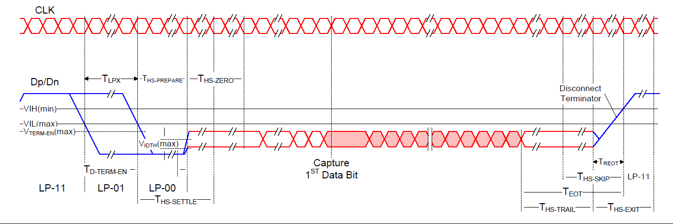
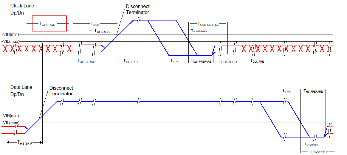
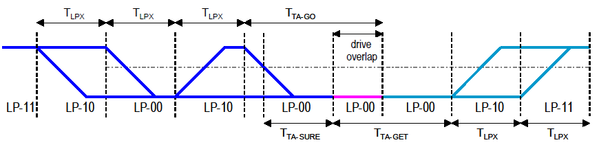
Note: If there are no special timing requirements, automatic calculation is currently supported m_wHsTrail, m_wHsPrpr, m_wHsZero, m_wDaHsExit, m_wClkTrail, m_wClkHsPrpr, m_wClkZero, m_wClkHsExit, m_wClkHsPost, m_wLpx, m_wTaGet, m_wTaSure, m_wTaGo, m_wContDet. These parameters can be left blank and automatically calculated by the code.
Note: The above dphy parameters are derived from MIPI_D-PHY_specification.pdf
| Parameters | Description |
|---|---|
| m_wHsTrail | T_{HS-TRAIL} (Reference file configuration MIPIDSIParamCalculation) |
| m_wHsPrpr | T_{HS-PREPARE} (Reference file configuration MIPIDSIParamCalculation) |
| m_wHsZero | T_{HS-ZERO} (Reference file configuration MIPIDSIParamCalculation) |
| m_wDaHsExit | T_{HS-EXIT} (Reference file configuration MIPIDSIParamCalculation) |
| Parameters | Description |
|---|---|
| m_wClkTrail | T_{CLK-TRAIL} (Reference file configuration MIPIDSIParamCalculation) |
| m_wClkHsPrpr | T_{CLK-PREPARE} (Reference file configuration MIPIDSIParamCalculation) |
| m_wClkZero | T_{CLK-ZERO} (Reference file configuration MIPIDSIParamCalculation) |
| m_wClkHsExit | T_{HS-EXIT} (Reference file configuration MIPIDSIParamCalculation) |
| m_wClkHsPost | T_{CLK-POST} (Reference file configuration MIPIDSIParamCalculation) |
| Parameters | Description |
|---|---|
| m_wLpx | T_{LPX} (Reference file configuration MIPIDSIParamCalculation) |
| m_wTaGet | T_{TA-GET} (Reference file configuration MIPIDSIParamCalculation) |
| m_wTaSure | T_{TA-SURE} (Reference file configuration MIPIDSIParamCalculation) |
| m_wTaGo | T_{TA-GO} (Reference file configuration MIPIDSIParamCalculation) |
| m_wContDet | contention detection, default 0 (Reference file configuration MIPIDSIParamCalculation) |
| m_wBllp | blanking or low power interval, default 0 |
| m_wFps | frame per second, follow panel spec |
| m_eLaneNum | data lane number, 1 ~ 4 |
| m_eFormat | data output format 0:RGB565 1:RGB666 2:LOOSELY_RGB666 3:RGB888 |
| m_eCtrlMode | 0:CMD_MODE 1:SYNC_PULSE 2:SYNC_EVENT 3:BURST_MODE |
| m_wDataClkSkew | default: 7 |
| m_ucPolCh0 | Channel 0 polarity 0:default 1:positive |
| m_ucPolCh1 | Channel 1 polarity 0:default 1:positive |
| m_ucPolCh2 | Channel 2 polarity 0:default 1:positive |
| m_ucPolCh3 | Channel 3 polarity 0:default 1:positive |
| m_ucPolCh4 | Channel 4 polarity 0:default 1:positive |
| m_ucClkLane | clk lane selection 0:select chn0 1:select chn1 2:select chn2 3:select chn3 4:select chn4 |
| m_ucDataLane0 | data lane0 selection 0:select chn0 1:select chn1 2:select chn2 3:select chn3 4:select chn4 |
| m_ucDataLane1 | data lane1 selection 0:select chn0 1:select chn1 2:select chn2 3:select chn3 4:select chn4 |
| m_ucDataLane2 | data lane2 selection 0:select chn0 1:select chn1 2:select chn2 3:select chn3 4:select chn4 |
| m_ucDataLane3 | data lane3 selection 0:select chn0 1:select chn1 2:select chn2 3:select chn3 4:select chn4 |
| m_ePacketType | MIPI LP cmd Data Type, default 0:DCS |
| m_pCmdBuff | MIPI panel cmd buffer, follow panel spec |
| m_pDeinitCmd | MIPI panel deinit cmd buffer, follow panel spec, content format is the same as m_pCmdBuff, delete this parameter if not needed |
m_ePacketType specifies the Data Type of m_pCmdBuff. 0 means DCS, 1 means GENERIC. Any other value is encapsulated into the packet as the actual Data Type value. Only decimal values are accepted as input.
Example: set the Data Type of the LP Cmd to 0x32 (Turn On Peripheral Command).
m_pCmdBuff is the panel initialization cmd. This part is customized by each panel manufacturer according to the protocol annotation. Therefore, the setting content of this parameter is generally provided by the panel manufacturer. The setting content format of this parameter is as follows, filled in hexadecimal.
"m_pCmdBuff":[
    "cmd1","data_num","data[0]","data[1]",...,"data[num-1]",
    ...,
    "cmdN","data_num","data[0]","data[1]",...,"data[num-1]",
    "0xFF","0xFF"  //Terminator
]
Note: "0xFE, 0xFE, 0xXX" in m_pCmdBuff means delay in ms
| Parameters | Description |
|---|---|
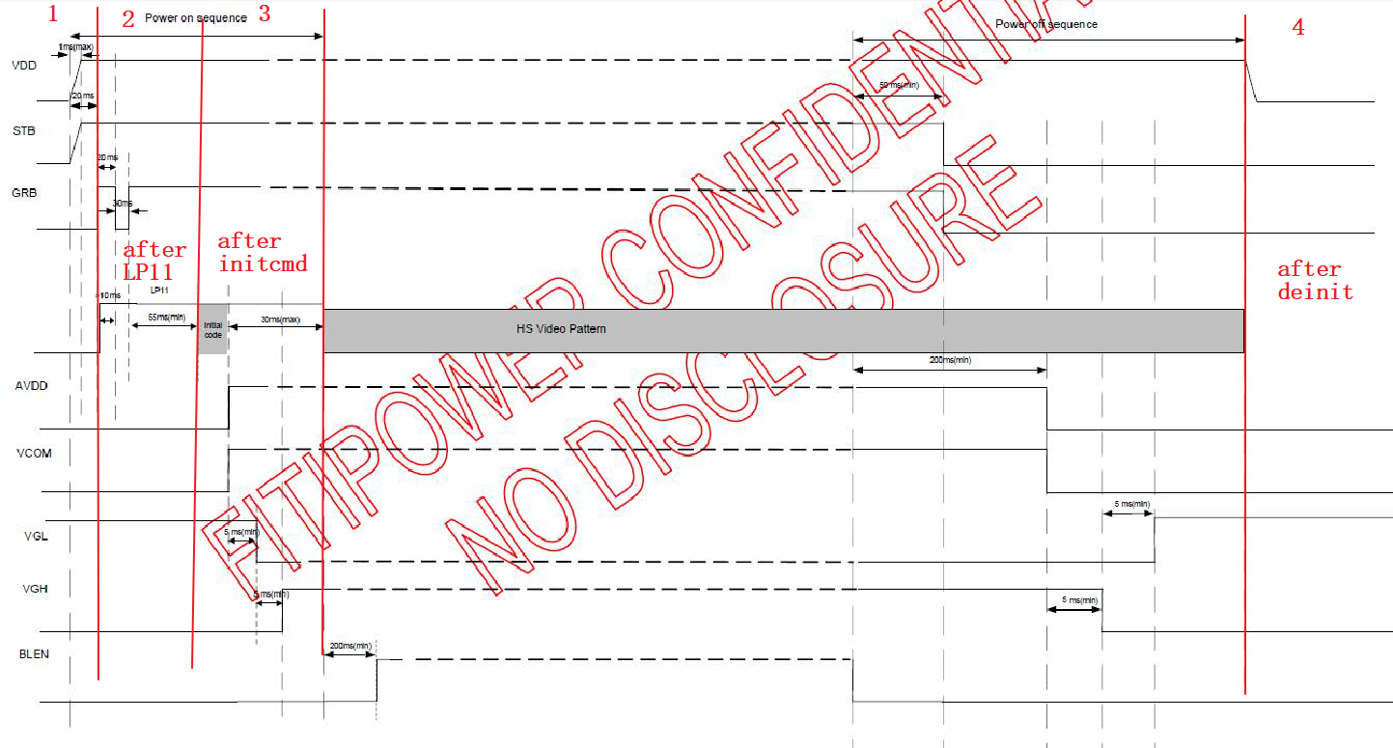
| m_pAfterLP11 | After LP11, power on timing control, delete this parameter if not needed |
| m_pAfterInit | After mipidsi init cmd is sent, power on timing control, if not needed, delete this parameter |
| m_pAfterDeinitCmd | After mipidsi deinit cmd is sent, power off timing control, if not needed, delete this parameter |
m_pAfterLP11, m_pAfterInit, and m_pAfterDeinitCmd are used to control the power-on and power-off timing of the screen. The content format is as follows. pin_idx must be followed by level and delay_ms, which are filled in decimal.
"m_pAfterLP11":[
    "pin_idx","level","delay_ms",
    "pin_idx","level","delay_ms",
    ...,
    "pin_idx","level","delay_ms"
]
Example: m_pAfterLP11: Pull up gpio_179 and delay for 10ms ->Pull down gpio_179 and delay for 10ms ->Pull up gpio_179 and delay for 10ms
4.4 LVDS Interface Specific Parameters
LVDS interface requires additional configuration of the following parameters, which default to 0 if not configured.
| Parameters | Description |
|---|---|
| lvds_eFormat | data format 0:VESA 1:JEIDA |
| lvds_eLaneNum | lane number 0:NONE 3:3 lane 4:4 lane |
| lvds_u8SwapOddEven | swap odd and even for dual-lvds 0:default 1:swap |
| lvds_u8SwapML | Swap RGB MSB/LSB 0:disable M/L swap 1:enable M/L swap |
| lvds_u8PolHsync | Hsync polarity |
| lvds_u8PolVsync | Vsync polarity |
| lvds_u8ClkLane | default: 0x63 |
| lvds_u8PolLane0 | lane0 polarity 0:default 1:positive |
| lvds_u8PolLane1 | lane1 polarity 0:default 1:positive |
| lvds_u8PolLane2 | lane2 polarity 0:default 1:positive |
| lvds_u8PolLane3 | lane3 polarity 0:default 1:positive |
| lvds_u8PolLane4 | lane4 polarity 0:default 1:positive |
| lvds_u8SwapLane0 | data lane0 selection 0:select chn0 1:select chn1 2:select chn2 3:select chn3 4:select chn4 |
| lvds_u8SwapLane1 | data lane1 selection 0:select chn0 1:select chn1 2:select chn2 3:select chn3 4:select chn4 |
| lvds_u8SwapLane2 | data lane2 selection 0:select chn0 1:select chn1 2:select chn2 3:select chn3 4:select chn4 |
| lvds_u8SwapLane3 | data lane3 selection 0:select chn0 1:select chn1 2:select chn2 3:select chn3 4:select chn4 |
| lvds_u8SwapLane4 | data lane4 selection 0:select chn0 1:select chn1 2:select chn2 3:select chn3 4:select chn4 |
5. Correct Configuration of Screen Parameters
To configure the screen parameters correctly, in addition to referring to the table attached to the above list, you also need to adjust the corresponding parameters according to the screen specifications or protocol specifications.
5.1 Screen Specifications
The Timing related section can be found in the specifications of most screen chips, as shown in the figure below. If you cannot find this information, please consult with the manufacturer.

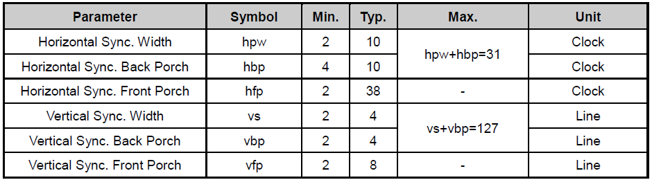
| Parameters | Descriptions |
|---|---|
| m_wPanelVSyncWidth | Horizontal Sync. Width |
| m_wPanelHSyncBackPorch | Horizontal Sync. Back Porch |
| m_wPanelVSyncWidth | Vertical Sync. Width |
| m_wPanelVBackPorch | Vertical Sync. Back Porch |
| m_wPanelHStart | m_wPanelHSyncWidth+m_wPanelHSyncBackPorch |
| m_wPanelVStart | m_wPanelVSyncWidth+m_wPanelVBackPorch |
| m_wPanelWidth | 240(H) |
| m_wPanelHeight | 320(V) |
| m_wPanelHTotal | m_wPanelHStart+m_wPanelWidth + hfp |
| m_wPanelVTotal | m_wPanelVStart+m_wPanelHeight + vfp |
5.2 Protocol Specification
If it is a MIPI panel, you also need to configure MIPI dphy related parameters according to the MIPI spec.
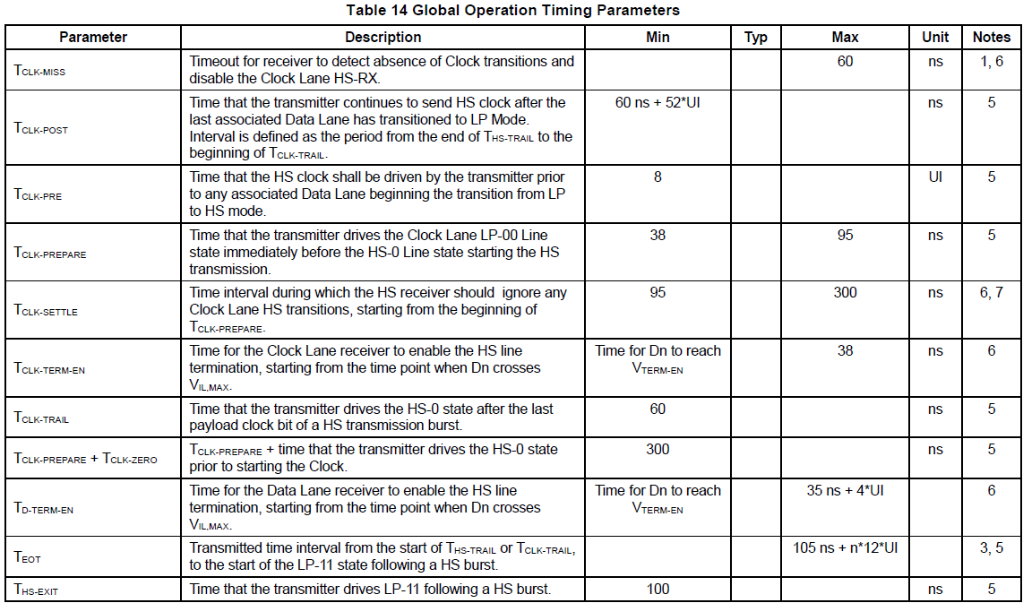
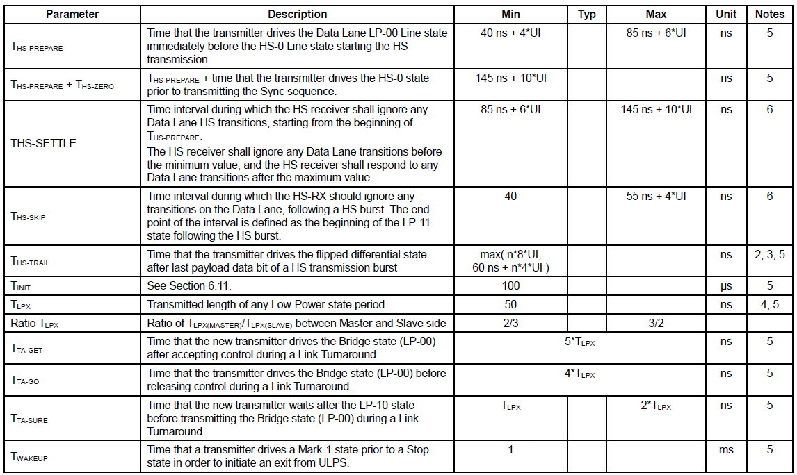
UI features:

H_Total = m_wPanelHTotal

V_Total = m_wPanelVTotal

BitsPerPixel=24(RGB888)/18(RGB666)/16(RGB565)

Bitrate = H_Total * V_Total * FPS * BitsPerPixel / lane number

UI = 1/Bitrate
For example, the HS-PREPARE requirement in the table is greater than (40ns + 4 * UI) and less than (85ns + 6 * UI), then the corresponding parameters in MIPI dphy timing are
(40ns + 4 * UI) / (8 * UI) < m_wHsPrpr < (85ns + 6 * UI) / (8 * UI)
The calculation methods for other MIPI dphy timing parameters are the same as above.
hpw, hbp, hfpmust satisfy the following formula
data_init_cycle = HsExit + Lpx + HsPrpr + HsZero

HFP_WC = HFP * BPP – 12 – data_init_cycle * lane_num

HBP_WC = HBP * BPP – 10

HSA_WC = HPW * BPP – 10

HFP_WC/HBP_WC/HSA_WC need > 0
The above parameter calculations can refer to the document MIPIDSIParamCalculation.