ADCLP USER GUIDE
REVISION HISTORY
| Revision No. | Description |
Date |
|---|---|---|
| 1.0 | 09/06/2024 | |
| 1.1 | 04/14/2025 | |
| 1.2 | 09/02/2025 |
1. OVERVIEW
The Successive Approximation ADC uses a feedback comparison circuit structure. The implementation method is briefly summarized as follows: take a digital quantity and add it to the DAC to get a corresponding output analog voltage. Compare this analog voltage with the input analog voltage signal. If the two are not equal, adjust the digital quantity until the two analog voltages are equal. The final digital quantity is the desired conversion result.
2. KEYWORD DESCRIPTION
-
ADCLP
Analog-to-digital converter Low Precision, low-precision (10-bit) analog-to-digital converter.
-
ADCMP
Analog-to-digital converter Medium Precision, medium-precision (12bit) analog-to-digital converter.
-
Upper/lower bound
ADCLP can set the upper and lower limits of the external input voltage digital quantity, and an interrupt will be triggered if it exceeds the range.
-
Reference voltage
The reference voltage used for analog-to-digital conversion calculations, which is also the maximum range. If the reference voltage is set to 1.8v, when the external input voltage is >=1.8v, the digital value reaches the maximum value of 1023.
3. FUNCTION DESCRIPTION
3.1. Hardware Function Description
-
SAR ADCLP has a total of 5 channels that can support analog-to-digital conversion of external input voltage.
-
The sampling accuracy is 10 bits, so the acquired register value range is 0~0x3ff.
-
Supports switching of two-level reference voltage (i.e. full scale), which are 1.8V and 1.0V respectively.
-
Supports threshold setting of external input voltage.
-
Sampling frequency = 12Mhz / 104 = 115384hz (equivalent to a sampling interval of 8667ns per point on the hardware).
3.2. Calculation instructions
The main function of SAR ADCLP is to convert analog signals into corresponding digital signals, that is, it can convert the input voltage into digital quantities and store them in registers, and calculate the input voltage through the formula.
Calculation formula: voltage = (register value / full scale) * reference voltage.
That is, if the value read is 0x1D2, the voltage is 0x1D2/0x3FF *1.8 = about 0.82v.
4. HARDWARE CONNECTION INTRODUCTION
As shown in the figure below, the external voltage can be connected to the pins PAD_SAR_GPIO0~PAD_SAR_GPIO4.
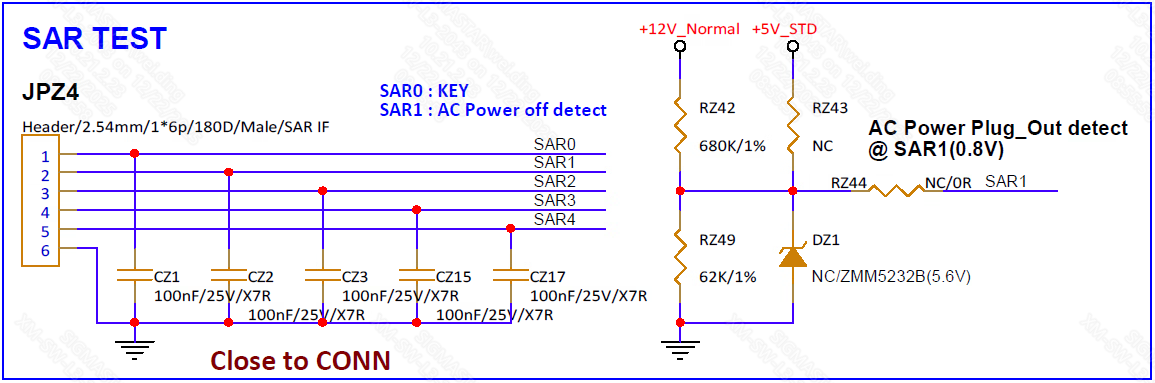
Figure 4-1: Adclp-1
5. UBOOT USAGE INTRODUCTION
5.1. Uboot Config Configuration
Check Kconfig to see that supporting ADCLP requires configuring CONFIG_SGS_ADCLP, CONFIG_ADC and CONFIG_CMD_ADC. To enable CONFIG_CMD_ADC, you need to configure CONFIG_DM_REGULATOR first.
-
CONFIG_SGS_ADCLP=y
-
CONFIG_ADC=y
-
CONFIG_DM_REGULATOR=y
-
CONFIG_CMD_ADC=y
5.2. DTS Configuration
The DTS configuration of SAR ADCLP only needs to configure the following information in chipname.dtsi:
adclp: adclp {
    compatible = "sgs,adclp";
    reg = <0x1F002800 0x200>;
    chan-num = <5>;
    ref-voltage = <1800>;
    status = "okay";
};
SAR ADCLP DTS configuration description:
| Attribute | Description | Setting Value | Remark |
|---|---|---|---|
| compatible | Match the driver to register the driver | "sgs,adclp" | Modification prohibited |
| reg | Set the register bank address | <0x1F002800 0x200> | Modification prohibited |
| chan-num | Set the number of channels supported | 5 | Modification prohibited |
| ref-voltage | Set the reference voltage level | In mv, 1800 and 1000 can be selected | Can be modified as needed |
| status | Select whether to enable the driver | "okay" or "disable" | Can be modified as needed |
5.3. Uboot cmd Parameter Description and Use Case
In command lines, input adc:
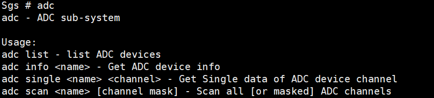
Figure 5-1: Adclp-6
(1) adc list -> check whether sar adclp is bound.

Figure 5-2: Adclp-7
(2) adc info adclp -> view the number of channels and data precision supported by sar adclp.
As shown below, the number of channels currently supported is 5 (note that the mask is 0x1f), and the maximum data value is 0x3ff.
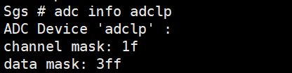
Figure 5-3: Adclp-8
(3) adc single adclp [channel] -> view the data of a specific channel.
As shown in the figure below, the value of channel 0 is 605.
According to the formula: voltage = (data / 0x3ff) * reference voltage.
At this time, the voltage is 605 / 1023 * 1.8 V = 1.065V.

Figure 5-4: Adclp-9
(4) adc scan adclp [channel mask] -> view the data of multiple channels.
adc scan adclp: view the data of all channels.
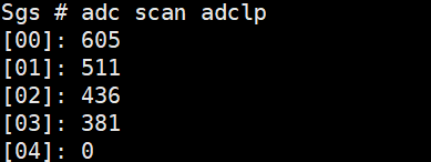
Figure 5-5: Adclp-10
adc scan adclp 0x3: -> view the data of channel 0 and channel 1.
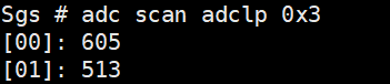
Figure 5-6: Adclp-11
5.4. Non-DM moderator framework Usage
In order to provide a higher degree of customization, the adclp driver can choose not to connect to the DM Regulator framework and directly implement the ADC sampling function through API calls. It only needs to set CONFIG and call the API in the header file.
5.4.1. CONFIG
-
CONFIG_ADC=n
-
CONFIG_SGS_ADCLP=y
5.4.2. API Description
Reference header filedrivers/sgs_common/include/drv_adclp.h
enum adclp_vdd_type
{
    ADCLP_VDD_CPU = 0,
    ADCLP_VDD_DLA,
    ADCLP_VDD_MIU,
    ADCLP_VDD_CORE,
    ADCLP_VDD_NODIE,
    ADCLP_VSS,
};

s32 drv_adclp_enable(u8 channel, u8 enable);
s32 drv_adclp_vdd_data(u8 channel, u16 *data, enum adclp_vdd_type type);
s32 drv_adclp_sample_data(u8 channel, u16 *data);
5.4.2.1. drv_adclp_enable
-
Objective
Enable sampling function
-
Syntax
s32 drv_adclp_enable(u8 channel, u8 enable); -
Parameter
Parameter Name Description channel Sampling channel enable enable status -
Return Value
Return Value Description 0 Success EINVAL Fail
5.4.2.2. drv_adclp_vdd_data
-
Objective
Get the VDD sampling result of the specified channel (only supports channel=8)
-
语法
s32 drv_adclp_vdd_data(u8 channel, u16 *data, enum adclp_vdd_type type); -
Syntax
Parameter Name Description channel Sampling channel (only supports channel=8), internal direct connection, PIN pin does not need external load data VDD_CPU、VDD_CORE and other sampling results type VDD_CPU、VDD_DLA、VDD_MIU、VDD_CORE -
Return Value
Return Value Description 0 Success EINVAL Fail
5.4.2.3. drv_adclp_sample_data
-
Objective
Get the external input voltage value of the specified channel
-
Syntax
s32 drv_adclp_sample_data(u8 channel, u16 *data) -
Parameter
Parameter Name Description channel Sampling channel data Sampling value -
Return Value
Return Value Description 0 Success EINVAL Fail
5.4.3. DEMO
#include <command.h>
#include <common.h>
#include <drv_adclp.h>

int do_adclp(struct cmd_tbl *cmdtp, int flag, int argc, char *const argv[])
{
    int   ret;
    char *cmd;
    u16 * data;
    u8    enable;
    u8    channel;

    cmd = argv[1];
    if (strcmp(cmd, "init") == 0)
    {
        if (argc != 4)
        {
            printf("adclp init [channel] [enable]\r\n");
            return CMD_RET_USAGE;
        }

        channel = (int)simple_strtoul(argv[2], NULL, 10);
        enable  = (int)simple_strtoul(argv[3], NULL, 10);

        ret = drv_adclp_enable(channel, enable);
        if (ret)
        {
            return CMD_RET_USAGE;
        }
    }
    else if (strcmp(cmd, "vdd") == 0)
    {
        if (argc != 3)
        {
            printf("adclp vdd [channel] \r\n");
            return CMD_RET_USAGE;
        }

        channel = (int)simple_strtoul(argv[2], NULL, 10);

        ret = drv_adclp_vdd_data(channel, data, ADCLP_VDD_CPU);
        if (ret)
        {
            return CMD_RET_USAGE;
        }
        printf("adclp channel[%d] data[%hu]\r\n", channel, *data);
    }
    else if (strcmp(cmd, "sample") == 0)
    {
        if (argc != 3)
        {
            printf("adclp sample [channel] \r\n");
            return CMD_RET_USAGE;
        }

        channel = (int)simple_strtoul(argv[2], NULL, 10);

        ret = drv_adclp_sample_data(channel, data);
        if (ret)
        {
            return CMD_RET_USAGE;
        }
        printf("adclp channel[%d] data[%d]\r\n", channel, *data);
    }
    else
    {
        printf("adclp command error\r\n");
        return CMD_RET_USAGE;
    }

    return 0;
}

static char adclp_help_text[] =
    "\n"
    "adclp init   [channel] [enable] \n"
    "adclp vdd    [channel]\n"
    "adclp sample [channel]\n";

U_BOOT_CMD(adclp, CONFIG_SYS_MAXARGS, 1, do_adclp, "adclp test", adclp_help_text);
6. KERNEL USAGE INTRODUCTION
6.1. Kernel Config Configuration
SAR ADCLP associated driver module Config:
- CONFIG_IIO
SAR ADCLP driver enable requires the following configuration:
Device Drivers --->

    [*] Sgs SoC platform drivers --->

        <*> Sgs ADCLP driver
6.2. DTS Configuration
The DTS configuration of SAR ADCLP only needs to configure the following information in chipname.dtsi:
adclp0: adclp0@1f002800 {
    compatible = "sgs,adclp";
    interrupts=<GIC_SPI INT_IRQ_SAR_ADC_WAKEUP IRQ_TYPE_LEVEL_HIGH>;
    reg = <0x0 0x1F002800 0x200>;
    clocks = <&CLK_sar>;
    interrupt-enable;
    channel = <0>;
    scope = <0>;
    ref-voltage = <1800>;
    upper-bound = <0x3FF>;
    lower-bound = <0>;
    #io-channel-cells = <0>;
    status = "ok";
};
| Attribute | Description | Setting Value | Remark |
|---|---|---|---|
| compatible | Match the driver to register the driver | "sgs,adclp" | Modification prohibited |
| interrupts | Set the interrupt | Modification prohibited | |
| reg | Set the register bank address | 0x1F002800 | Modification prohibited |
| clocks | Set the clock source | &CLK_sar | No modification required |
| interrupt-enable | Enable the interrupt | bool type, the comment means disable | Can be modified as needed |
| channel | Set the channel | 0~4 | No modification required |
| scope | Set the scope | As a channel for measuring external input voltage, scope are all 0 | Can be modified as needed |
| ref-voltage | Set the reference voltage level | In mv, 1800 and 1000 can be selected | Can be modified as needed |
| upper-bound | Set the upper threshold voltage | 0~0x3FF, enable interrupt | Can be modified as needed |
| lower-bound | Set the lower threshold voltage | 0~0x3FF, enable interrupt | Can be modified as needed |
| status | Whether to enable the driver | "ok" or "disable" | Can be modified as needed |
6.3. Padmux Configuration
SAR-ADCLP does not require padmux configuration, and the PIN pins on the schematic diagram will be configured as ADC sampling function by default, but if the SAR_GPIO pins are configured as GPIO MODE in padmux.dtsi, the ADC function will be disabled.
6.4. Module Usage Introduction
6.4.1 SYSFS Interface Description
-
Enter SAR ADCLP sampling channel Channel 0
cd /sys/class/sgs/adclp0/ -
Set the threshold of SAR ADCLP0 (sampling will not be affected if the threshold is not set)
echo 800 400 > /sys/class/sgs/adclp0/threshold (The first parameter 800 is the upper threshold, and the second parameter 400 is the lower threshold. That is, an ADC code within the threshold range of 400~800 is considered safe; values outside this range will trigger an interrupt. You can refer to the implementation in kernel/drivers/sgs_common/adc/ut/lnx/adclp_lnx_ut.c. This parameter only serves for threshold configuration—the interrupt callback needs to be implemented by your program. Therefore, when verifying the SYSFS interface, this parameter can be omitted.) -
Enable SAR ADCLP0
echo 1 > enable -
Get the digital quantity after SAR ADCLP0 sampling
cat /sys/class/sgs/adclp0/value
6.4.2. IIO Interface Description
-
Enter the IIO entry of ADCLP channel
cd /sys/bus/iio/devices/iio:adclp0 //Entrance to channel 0 cd /sys/bus/iio/devices/iio:vdd-mux //Entrance to VDD channel cd /sys/bus/iio/devices/iio:tsensor //Entrance to Tsensor channel -
Set the type of VDD or Tsensor (only supports iio:vdd-mux and iio:tsensor)
echo N > in_voltage_phase //N is adclp_vdd_type or adclp_tsensor_type -
Enable channel
echo 1 > in_voltage_en -
Get the ADC code of the channel
cat in_voltage_raw -
Get the calculated scale factor of the channel
in_voltage_scale
Actual voltage = in_voltage_raw value * in_voltage_scale value
6.4.3 Ioctl Interface Description
The header File<drv_adclp.h> is located in the kernel/drivers/sgs_common/include directory.
-
IOCTL_ADCLP_SET_BOUND
Set the sampling voltage threshold.
-
IOCTL_ADCLP_READ_VALUE
Get the digital quantity after voltage conversion.
struct adclp_bound
{
    u16 upper_bound;
    u16 lower_bound;
};

#define ADCLP_IOC_MAXNR        1
#define ADCLP_IOC_MAGIC        'a'
#define IOCTL_ADCLP_SET_BOUND  _IO(ADCLP_IOC_MAGIC, 0)
#define IOCTL_ADCLP_READ_VALUE _IO(ADCLP_IOC_MAGIC, 1)
6.5. Sample Code
6.5.1 Ioctl
The source code is located in kernel/drivers/sgs_common/adc/ut/lnx/adclp_lnx_ut.c
#include <fcntl.h>
#include <stdio.h>
#include <errno.h>
#include <signal.h>
#include <stdlib.h>
#include <unistd.h>
#include <string.h>
#include <limits.h>
#include <sys/stat.h>
#include <sys/ioctl.h>
#include <sys/types.h>
#include <drv_adclp.h>

void sample_warn(int num)
{
    printf("adclp data exceeding the threshold\n");
}

int get_parameter(u16 *para, const char *str)
{
    long  value  = 0;
    char *endptr = NULL;

    errno = 0;
    value = strtol(str, &endptr, 0);

    if (errno == ERANGE)
    {
        fprintf(stderr, "Error: parameter '%s' out of range [%ld, %ld]\n", str, LONG_MIN, LONG_MAX);
        return -ERANGE;
    }
    if (endptr == str)
    {
        fprintf(stderr, "Error: parameter '%s' not a valid number\n", str);
        return -EINVAL;
    }
    if (*endptr != '\0')
    {
        fprintf(stderr, "Warning: parameter '%s' contains extra characters '%s'\n", str, endptr);
    }

    if (value > UINT_MAX)
    {
        fprintf(stderr, "Error: value %ld greater than [%u]\n", value, UINT_MAX);
        return -EINVAL;
    }

    *para = (u16)value;

    return 0;
}

int main(int argc, char **argv)
{
    int                i;
    int                fd;
    int                ret;
    char               cmd;
    int                flags;
    u16                value;
    u16                channel;
    u16                upper_bd;
    u16                lower_bd;
    u16                chan_num;
    char               path[64];
    struct adclp_bound adclp_bd;

    if (argc < 2)
    {
        printf("format: adclp_lnx_ut once [channel] <upper> <lower>\n");
        printf("format: adclp_lnx_ut scan [chan num]\n");
        return -1;
    }

    if (!strcmp(argv[1], "once"))
    {
        if (argc == 3)
        {
            ret = get_parameter(&channel, argv[2]);
            if (ret < 0)
            {
                return ret;
            }
        }
        else if (argc == 5)
        {
            ret = get_parameter(&channel, argv[2]);
            if (ret < 0)
            {
                return ret;
            }

            ret = get_parameter(&upper_bd, argv[3]);
            if (ret < 0)
            {
                return ret;
            }
            adclp_bd.upper_bound = (u16)upper_bd;

            ret = get_parameter(&lower_bd, argv[4]);
            if (ret < 0)
            {
                return ret;
            }
            adclp_bd.lower_bound = (u16)lower_bd;
        }
        else
        {
            printf("format: adclp_lnx_ut once [channel] <upper> <lower>\n");
            return -1;
        }

        snprintf(path, sizeof(path), "/dev/adclp%u", channel);
        fd = open((const char *)(char *)path, O_RDWR);
        if (fd < 0)
        {
            printf("open device fail\n");
            return -1;
        }

        if (argc == 5)
        {
            ioctl(fd, IOCTL_ADCLP_SET_BOUND, &adclp_bd);
        }

        signal(SIGIO, sample_warn);

        fcntl(fd, F_SETOWN, getpid());
        flags = fcntl(fd, F_GETFL);
        fcntl(fd, F_SETFL, flags | FASYNC);

        while (1)
        {
            cmd = getchar();
            if (cmd == 'q' || cmd == 'Q')
            {
                break;
            }

            ioctl(fd, IOCTL_ADCLP_READ_VALUE, &value);
            printf("adclp%u data[%hu]\n", channel, value);
        }

        close(fd);
    }
    else if (!strcmp(argv[1], "scan"))
    {
        if (argc == 3)
        {
            ret = get_parameter(&chan_num, argv[2]);
            if (ret < 0)
            {
                return ret;
            }
        }
        else
        {
            printf("format: adclp_lnx_ut scan [chan num]\n");
            return -1;
        }

        for (i = 0; i < chan_num; i++)
        {
            snprintf(path, sizeof(path), "/dev/adclp%u", i);
            fd = open((const char *)(char *)path, O_RDWR);
            if (fd < 0)
            {
                printf("open device fail\n");
                continue;
            }

            ioctl(fd, IOCTL_ADCLP_READ_VALUE, &value);
            printf("adclp%u data[%hu]\n", i, value);
            close(fd);
        }
    }
    else
    {
        printf("format: adclp_lnx_ut once [channel] <upper> <lower>\n");
        printf("format: adclp_lnx_ut scan [chan num]\n");
        return -1;
    }

    return 0;
}
6.5.2 Kernel Mode
#include <linux/kernel.h>
#include <linux/module.h>
#include <linux/moduleparam.h>
#include <linux/platform_device.h>
#include <linux/of.h>
#include <drv_adclp.h>

static adclp_cb_t cb_t[4];

int adclp_get_data2(u8 channel)
{
    u16 data;

    drv_adclp_sample_data(channel, &data);
    printk("%s adclp test chan[%d], data[%hu]\n", __func__, channel, data);

    return 0;
}

int adclp_get_data1(u8 channel)
{
    u16 data;

    drv_adclp_sample_data(channel, &data);
    printk("%s adclp test chan[%d], data[%hu]\n", __func__, channel, data);

    return 0;
}

static int __init adclp_test_init(void)
{
    int ret;

    cb_t[0] = adclp_get_data1;
    ret = drv_adclp_register_callback(0, cb_t[0]);
    if (ret)
    {
        printk("adclp ch0-0 register callback fail\n");
        return ret;
    }

    cb_t[1] = adclp_get_data2;
    ret = drv_adclp_register_callback(0, cb_t[1]);
    if (ret)
    {
        printk("adclp ch0-1 register callback fail\n");
        return ret;
    }

    cb_t[2] = adclp_get_data1;
    ret = drv_adclp_register_callback(1, cb_t[2]);
    if (ret)
    {
        printk("adclp ch1-0 register callback fail\n");
        return ret;
    }

    cb_t[3] = adclp_get_data2;
    ret = drv_adclp_register_callback(1, cb_t[3]);
    if (ret)
    {
        printk("adclp ch1-1 register callback fail\n");
        return ret;
    }

    ret = drv_adclp_set_bound(0, 800, 600);
    if (ret)
    {
        printk("adclp ch0 set bound fail\n");
        return ret;
    }

    ret = drv_adclp_set_bound(1, 1000, 600);
    if (ret)
    {
        printk("adclp ch1 set bound fail\n");
        return ret;
    }

    drv_adclp_enable(0, 1);
    drv_adclp_enable(1, 1);

    return 0;
}

static void __exit adclp_test_exit(void)
{
    drv_adclp_enable(0, 0);
    drv_adclp_enable(1, 0);

    drv_adclp_unregister_callback(0, cb_t[0]);
    drv_adclp_unregister_callback(0, cb_t[1]);
    drv_adclp_unregister_callback(1, cb_t[2]);
    drv_adclp_unregister_callback(1, cb_t[3]);
}

module_init(adclp_test_init);
module_exit(adclp_test_exit);
7. API Reference
The API can refer to header file <drv_adclp.h> located in the kernel/drivers/sgs_common/include directory.
enum adclp_vdd_type
{
    ADCLP_VDD_CPU = 0,
    ADCLP_VDD_DLA,
    ADCLP_VDD_MIU,
    ADCLP_VDD_CORE,
    ADCLP_VDD_NODIE,
    ADCLP_VSS,
};

enum adclp_tsensor_type
{
    ADCLP_TSNR_SAR = 0,
    ADCLP_TSNR_CPU,
    ADCLP_TSNR_DLA,
    ADCLP_TSNR_CORE,
};

typedef s32 (*adclp_cb_t)(u8 channel);

//This function module provides the following kernel state interfaces
s32 drv_adclp_enable(u8 channel, u8 enable);
s32 drv_adclp_set_bound(u8 channel, u16 upper_bound, u16 lower_bound);
s32 drv_adclp_vdd_data(enum adclp_vdd_type type, u16 *data);
s32 drv_adclp_tsensor_data(enum adclp_tsensor_type type, u16 *data);
s32 drv_adclp_sample_data(u8 channel, u16 *data);
s32 drv_adclp_register_callback(u8 channel, adclp_cb_t cb_t);
s32 drv_adclp_unregister_callback(u8 channel, adclp_cb_t cb_t);
drv_adclp_enable
-
Purpose
Enable sampling function of the specified channel.
-
Syntax
s32 drv_adclp_enable(u8 channel, u8 enable) -
Parameter
Parameter Name Description channel Sampling channel enable Whether to enable -
Return Value
Return Value Description 0 Success -EINVAL Channel not supported
drv_adclp_set_bound
-
Purpose
Set the threshold of the specified channel.
-
Syntax
s32 drv_adclp_set_bound(u8 channel, u16 upper_bound, u16 lower_bound) -
Parameter
Parameter Name Description channel Sampling channel upper_bound Upper threshold lower_bound Lower threshold -
Return Value
Return Value Description 0 Success -EINVAL Channel not supported
drv_adclp_vdd_data
- Purpose
Get the ADC code of different VDD types without external input voltage. The ADC code value depends on the type passed in by adclp_vdd_type.
-
Syntax
s32 drv_adclp_vdd_data(enum adclp_vdd_type type, u16 *data) -
Parameter
Parameter Name Description type VDD Type data Pointer address to obtain sampling data -
Return value
Return value Description 0 Success -EINVAL Channel not supported
drv_adclp_tsensor_data
- Purpose
Get the ADC code of different tsensor types without external input voltage. The ADC code value depends on the type passed in by adclp_tsensor_type.
-
Syntax
s32 drv_adclp_tsensor_data(enum adclp_tsensor_type type, u16 *data) -
Parameter
Parameter Name Description type Tsensor Type data Pointer address to obtain sampling data -
Return value
Return value Description 0 Success -EINVAL Channel not supported
drv_adclp_sample_data
-
Purpose
Get the external input voltage digital quantity of the specified channel.
-
Syntax
s32 drv_adclp_sample_data(u8 channel, u16 *data); -
Parameter
Parameter Name Description channel Sampling channel data Pointer address to obtain sampling data -
Return Value
Return Value Description 0 Success -EINVAL Channel not supported
drv_adclp_register_callback
-
Purpose
Register the callback function of the specified channel (supports registering multiple callback functions for the same channel). When the sampling result exceeds the threshold, the callback function can be used to perform corresponding processing.
-
Syntax
s32 drv_adclp_register_callback(u8 channel, adclp_cb_t cb_t); -
Parameter
Parameter Name Description channel Sampling channel cb_t Function pointer -
Return Value
Return Value Description 0 Register successfully -EINVAL Register failed
drv_adclp_unregister_callback
-
Purpose
Release the callback function of the specified channel and the memory applied during registration.
-
Syntax
drv_adclp_unregister_callback(u8 channel, adclp_cb_t cb_t) -
Parameter
Parameter Name Description channel Sampling channel cb_t Function pointer -
Return Value
Return Value Description 0 Unregister successfully -EINVAL Unregister failed
8. FAQ
Q1:SAR ADCLP Interface Does Not Exist
-
Check if the
statusof the DTS ADCLP node isok -
Check if the kernel config is configured, see [6.1. Kernel Config Configuration]
Q2: The external input voltage changes, but the SAR ADCLP sampling data does not change
-
When the PIN is in GPIO MODE, the sampling data will not change. You can read the register value to determine whether the PIN is switched to GPIO MODE:
0x14 0x11 BIT0-BIT5: Each BIT of BIT0~BIT5 corresponds to a channel. When value=0, the PIN pin of the channel is in GPIO MODE. When value=1, the PIN pin of the channel is in ADC MODE. For example, when BIT0=0, channel 0 is in GPIO MODE. When BIT1=1, channel 1 is in ADC MODE. 0x14 0x11 BIT8-BIT13: Each BIT of BIT8~BIT13 corresponds to a channel. The prerequisite is that the PIN pin is in GPIO MODE. When value=0, the PIN pin is switched to output. When value=1, the PIN pin is switched to input. 0x14 0x12 BIT0-BIT5: Each BIT of BIT0~BIT5 corresponds to a channel. The prerequisite is that the PIN pin is in GPIO MODE and is set to ouput. When value=0, the PIN pin of the channel is switched to a low level. When value=1, the PIN pin of the channel is switched to a high level. For example: riu_r 0x14 0x11 Return value: 0x3F3F -> All channels are in ADC MODE Return value: 0x3E3E -> Channel 0 is in GPIO MODE, and the rest of the channels are in ADC MODE Return value: 0x0000 -> All channels are in GPIO MODE and switched to output -
When the PIN pin register is set to non-GPIO MODE, the sampled data still does not change. You can set the PIN pin to GPIO MODE and perform an output high/low test. If the PIN pin level cannot be pulled up or down, it can be judged as a hardware problem.
Q3: The first or first few sampling data have a large deviation from the actual input voltage
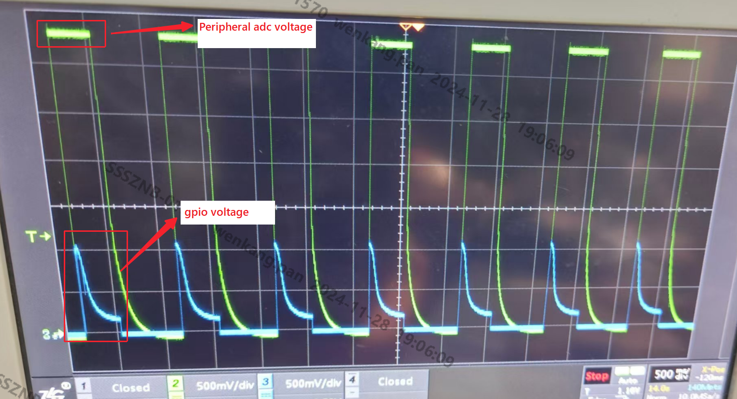
This problem is most likely related to the sampling timing. You can use GPIO as a trigger source to obtain the voltage status of the component at each sampling.
As shown in the figure below, before triggering ADC sampling, GPIO switches from high level to low level. The ADC sampling timing is just in the process of voltage decline, not when the voltage is stable. Therefore, it is judged as sampling abnormality. At this time, it is necessary to wait until the component is stable before sampling.