sdcard_sdio_debugsop Manual
REVISION HISTORY
| Revision No. | Description |
Date |
|---|---|---|
| 1.0 | 02/21/2024 |
1. SD/SDIO Card Identification Process Issues
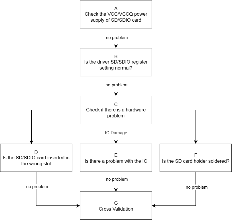
| Process | Method | Exit Conditions | Next Step | Information to Provide to SWRD | Related FAQs |
|---|---|---|---|---|---|
| A | 1. Use a multimeter to confirm whether the VCC voltage during the initialization phase of the SD card is 3.3V; confirm whether the VCCQ (IO) voltage meets the specifications according to the SDIO device user manual, generally SDIO devices can support a range of 1.7V to 3.6V, the VCC voltage is determined based on the actual situation of the SDIO device, and the manufacturer will provide a user manual. 2. Confirm that the default state of the CLK line is low and the CMD/Data line is high. 3. Confirm whether the VCCQ voltage of the SD/SDIO is within the range of 1.8/3.3V. |
Exit Condition 1: 1. The VCC power supply of the SD card during the initialization phase is significantly different from 3.3V, or the VCC power supply of the SDIO card does not meet the manual specifications. 2. Or the default state of the bus line is incorrect. 3. Or the VCCQ power supply of the SD/SDIO card is not within the effective range of 1.8/3.3V. > Power Supply Issue Exit Condition 2: Power supply is normal. > No Issues |
Exit Condition 1: > Process Ends Exit Condition 2: > B |
Exit Condition 1: ==> Seek CAE Assistance |
|
| B | 1. Confirm whether the padmux configuration of the SD/SDIO corresponds to the development board, and whether the pads conflict with other modes. Confirmation method: cd vim arch/arm/boot/dts/(chip name)_xxxx-padmux.dtsi The SD/SDIO padmux mode will have the keywords 'SD_BOOT_MODE' or 'SDIO_MODE', and the corresponding GPIO pads need to be confirmed for reuse with other modules. 2. Confirm whether the DTS related configuration of the SD/SDIO matches the currently used slot. Confirmation method: cd vim arch/arm/boot/dts/(chip name).dtsi For the meaning of related configuration items, please refer to 2.1 no-sdio/no-sd/no-mmc, if these three configuration items connect to which type of device, comment out the corresponding item and configure the other two, for example: if connecting an SD card, comment out no-sd and configure no-sdio/no-mmc. |
Exit Condition 1: 1. Padmux is not correctly configured or there is a conflict with other modes. 2. The related configuration items of SD/SDIO in the DTS do not match the currently used slot. > Configuration Error Issue Exit Condition 2: Configuration is normal. > No Issues |
Exit Condition 1: > Process Ends Exit Condition 2: > C |
Exit Condition 1: ==> Seek CAE to confirm the current padmux situation of the development board, and then configure the correct padmux and DTS according to the actual situation. |
|
| C | 1. Confirm whether there are hardware issues. 1.1. Scenario 1 - Wrong Slot: When the development board has multiple slots, connect according to the actual padmux. 1.2. Scenario 2 - IC Pin Output Unstable: Use a multimeter or oscilloscope to measure signals near the IC side and near the device side; there should be no signal instability. 1.3. Scenario 3 - SD Card Socket Cold Solder: If no issues are found with other conditions, try using a small SD card socket in the same slot; if there are no issues, try re-soldering the SD card socket. |
Exit Condition 1: 1. Confirm the SD card is inserted in the wrong slot. > Insert into the correct slot. Exit Condition 2: IC pin output is unstable, leading to poor signal quality. > Replace with a new IC. Exit Condition 3: SD card socket cold solder, leading to poor signal quality. > Re-solder the SD card socket. Exit Condition 4: Hardware is normal. > No Issues |
Exit Condition 1: > Process Ends Exit Condition 2: > Process Ends Exit Condition 3: > Process Ends Exit Condition 4: > G |
Exit Condition 2: > Seek CAE Assistance Exit Condition 3: > Seek CAE Assistance |
|
| G | 1. Replace with an SD/SDIO card of the same specification and test again to see if it is recognized normally. 2. Replace the development board and test whether the SD/SDIO card of the same specification is recognized normally. 3. Test the SD/SDIO card of the same specification on other platforms to see if it is recognized normally. |
Exit Condition 1: After replacing with an SD/SDIO card of the same specification, it can be recognized normally. > SD/SDIO Device Issue. Exit Condition 2: After testing with a replaced development board, it can be recognized normally. > Development Board Issue. Exit Condition 3: After testing on other platforms, it can be recognized normally. ==> Driver Issue. |
Exit Condition 1: > Process Ends Exit Condition 2: > Process Ends Exit Condition 3: ==> Process Ends |
Exit Condition 3: >1. Provide serial log. >2. Use LA or oscilloscope to capture the waveform of the entire initialization process. ==>3. In the Linux console, use the RIU command to dump the relevant bank information of the SDIO IP: 0x1413/0x1038/0x103C/0x103E |
2. SD/SDIO Communication Process Issues
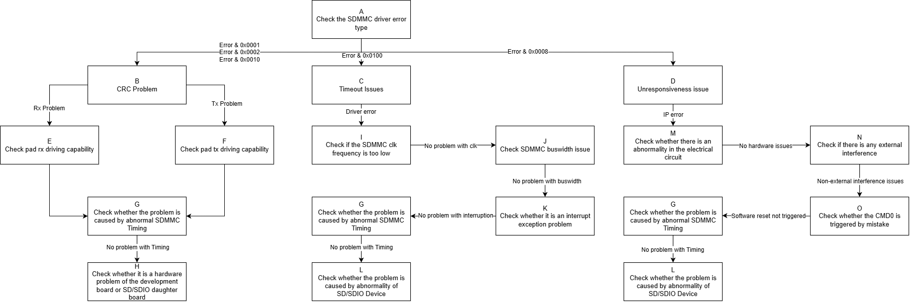
| Process | Method | Exit Conditions | Next Step | Information to be Provided to SWRD | Related Reference FAQ |
|---|---|---|---|---|---|
| A | When an error occurs, retrieve the debug log based on the keyword "[sdmmc", mainly focusing on error numbers: 1.(E: 0x0001): read crc 2.(E: 0x0002): write crc 3.(E: 0x0010): cmd rsp crc 3.(E: 0x0100): driver reports timeout 4.(E: 0x0008): IP reports device no rsp |
Exit Condition 1: 1.cmd 12/13/17/18/23/24/25/52/53 and other read/write related commands report crc errors Exit Condition 2: 1.cmd 12/13/17/18/23/24/25/52/53 and other read/write related commands report timeout errors Exit Condition 3: 1.cmd 12/13/17/18/23/24/25/52/53 and other read/write related commands report device not responding errors |
Exit Condition 1: >B Exit Condition 2: >C Exit Condition 3: ==>D |
||
| B | The essence of the crc issue is poor signal quality. The best driving capability of the pad can be selected based on the type of crc error and combined with adjustments to driving (the range for GPIOE pads is 0-1, and for GPIOA pads is 0-3) | Exit Condition 1: 1.crc error type is rx crc, i.e., an error occurs during reading Exit Condition 2: 1.crc error type is tx crc, i.e., an error occurs during writing Exit Condition 3: 1.other crc error types |
Exit Condition 1: >E Exit Condition 2: >F Exit Condition 3: ==>G |
||
| C | 1. For timeout issues during driver read/write operations, capture waveforms immediately to confirm whether there are transmission performance issues 2. If there are no issues with the waveforms, determine whether the sdmmc MIE interrupt is reported or received normally 3. Check if there are any abnormalities in sdmmc timing 4. If there are no issues in the above situations, consider whether the sd/sdio device is abnormal |
Exit Condition 1: 1. According to the waveform, the current working frequency is lower than expected Exit Condition 2: 1. Check if the bus width is inconsistent with expectations Exit Condition 3: 1. According to the debug log, the relevant event did not trigger normally when an error occurred Exit Condition 4: 1. sdmmc timing is abnormal Exit Condition 5: 1. sd/sdio device causes card busy situation |
Exit Condition 1: >I Exit Condition 2: >J Exit Condition 3: >K Exit Condition 4: >G Exit Condition 5: ==>L |
||
| D | 1. For the sdmmc IP reporting device no response issues, capture waveforms to confirm whether the cmd was sent without receiving a response 2. Refer to <1: sd/sdio card identification process issues>, check if the relevant configurations are correct 3. Prioritize checking whether the hardware electrical path is normal and whether the operating environment is subjected to interference tests (such as electrostatic discharge, high and low temperature, etc.) 4. Search the debug log for the keyword "SAR1 SDMMC WARN trigger" to determine if there is a case of power-off protection being triggered incorrectly 5. Check if there are any abnormalities in sdmmc timing 6. If there are no issues in the above situations, consider whether the sd/sdio device is abnormal |
Exit Condition 1: 1. Check if the configuration is correct; the waveform shows that after the cmd is sent, no device response is received Exit Condition 2: 1. Check if there is significant signal attenuation in the electrical path between the chip and the sd/sdio device sub-board Exit Condition 3: 1. The operating environment is currently undergoing electrostatic discharge or high and low temperature stress testing Exit Condition 4: 1. Search the log and find that sdmmc has triggered power-off protection without power-off Exit Condition 5: 1. sdmmc timing is abnormal Exit Condition 6: 1. sd/sdio device causes non-response situation Exit Condition 7: 1. The waveform shows that the device is responsive, but the IP judges it as unresponsive |
Exit Condition 1: >Process Ends Exit Condition 2: 1. Please assist CAE in troubleshooting Exit Condition 3: >Process Ends Exit Condition 4: >Process Ends Exit Condition 5: >G Exit Condition 6: >L Exit Condition 7: >Process Ends |
Exit Condition 1: 1. Dump debug log and DTS configuration file Exit Condition 3: Exit Condition 4: 1. Dump debug log Exit Condition 7: 1. Expected CHIP design defect |
|
| E | Adjust driving (the range for GPIOE pads is 0-1, and for GPIOA pads is 0-3) | Exit Condition 1: 1. After setting the data driving level according to the actual situation, it returns to normal Exit Condition 2: 1. After trying all data driving levels, crc errors still occur |
Exit Condition 1: >Process Ends Exit Condition 2: >G |
||
| F | Adjust driving (the range for GPIOE pads is 0-1, and for GPIOA pads is 0-3) | Same as "E" | Same as "E" | ||
| G | 1. Adjust driving (the range for GPIOE pads is 0-1, and for GPIOA pads is 0-3) to comprehensively adjust the driving capability of clk/cmd lines 2. Adjust clk phase; 3. Adjust the clock signal sampling mode according to the tmux table and sd/sdio reg table; 4. When using DMA in trans-mode, set reg_dma_rd_clk_stop to avoid data loss 5. Use LA or an oscilloscope to capture the complete waveform during the problematic phase |
Exit Condition 1: 1. After comprehensively adjusting the driving levels of the signal lines, it returns to normal Exit Condition 2: 1. After adjusting the clk's four-phase or eight-phase, it returns to normal Exit Condition 3: 1. After adjusting the clock signal sampling mode, it returns to normal Exit Condition 4: 1. In the DMA mode transmission scenario, set offset:0xb bit7 to return to normal Exit Condition 5: 1. None of the above measures are effective; the waveform differs from the normal waveform, such as insufficient rise time sampling lock time, cmd overlap, cmd minimum interval not met, etc. Exit Condition 6: 1. Confirm that all the above settings are normal and the waveform is without anomalies |
Exit Condition 1: Exit Condition 2: Exit Condition 3: Exit Condition 4: >Process Ends Exit Condition 5: >Process Ends Exit Condition 6: ==>H/L |
Exit Condition 5: 1. Dump the complete debug log of the entire process, including logs from sd/sdio init to the occurrence of the problem 2. Capture the complete waveform of the abnormal scenario, preferably with a normal scenario waveform under the same conditions for comparison 3. Use the riu command in the Linux console to dump the relevant bank information of the sdmmc IP: 0x1413/0x1038/0x103C/0x103E |
|
| H | 1. First refer to the cross-validation section of 2. In the default state (i.e., no data interaction), use a multimeter or oscilloscope to measure the electrical signals of the sd/sdio clk/cmd/data lines to see if they meet expectations 3. In the case of communication triggering (i.e., data interaction), use a multimeter or oscilloscope to measure the electrical signals near the chip end and near the device end to see if there are significant signal differences 4. Try to enhance driving capability from a hardware perspective by adding pull-up resistors and other means |
Exit Condition 1: 1. After cross-validation, communication returns to normal Exit Condition 2: 1. Under default conditions, clk line is not low, cmd/data lines are not high Exit Condition 3: 1. There are attenuation or other abnormal phenomena in the electrical signals between the IC end and the device end Exit Condition 4: 1. After adjusting the electrical signal quality from the hardware side, communication returns to normal Exit Condition 5: 1. Electrical signals are normal, and hardware adjustments have no effect |
Exit Condition 1: >Process Ends Exit Condition 2: 1. Check if the padmux configuration is consistent with the current sd/sdio slot being used 2. Use LA or an oscilloscope in Linux to manually pull up or down the sd/sdio pin gpio to see if it meets expectations Exit Condition 3: Exit Condition 4: Exit Condition 5: >Process Ends |
Exit Condition 3: 1. Seek CAE assistance Exit Condition 5: 1. Synchronize hardware conditions to help RD build a reproduction environment |
|
| I | 1. Clarify the version of the sd/sdio IP used in the current slot according to the manual 1.1 sd/sdio 2.0 supports a maximum of 48MHz 1.2 sd/sdio 3.0 supports a maximum of 200MHz 2. Confirm whether it is already at the highest level within the frequency range allowed by the IP 3. Read bank 0x1038 offset 0x43/bank 0x42 offset 0x24 to confirm whether clk is set successfully as expected 4. Refer to |
Exit Condition 1: 1. Adjust clk to the highest level, communication returns to normal Exit Condition 2: 1. Adjusting clk has no effect or is already at the highest level Exit Condition 3: 1. clk setting does not match the register read value |
Exit Condition 1: >Process Ends Exit Condition 2: >J Exit Condition 3: ==>Process Ends |
Exit Condition 3: 1. Dump 0x1038/0x1133 register information 2. Provide dts configuration file 3. Provide debug log |
|
| J | 1. According to the SPEC document, different speed modes have corresponding supported bus widths 1.1 sd/sdio 2.0 can use 1bit/4bit Buswidth 1.2 sd/sdio 3.0 can only use 4bit width 2. Read bank 0x1413/0x42 offset 0xb[2:1] to confirm |
Exit Condition 1: 1. Adjust bus width to the maximum width corresponding to the speed mode, communication returns to normal Exit Condition 2: 1. Adjusting bus width has no effect or is already at the maximum width for that speed mode Exit Condition 3: 1. bus width setting does not match the register read value |
Exit Condition 1: >Process Ends Exit Condition 2: >K Exit Condition 3: ==>Process Ends |
Exit Condition 3: 1. Dump 0x1413/0x42 register information 2. Provide dts configuration file 3. Provide debug log |
|
| K | 1. Read bank 0x1413 offset 0x0[1:0] to determine whether the read/write complete event has been raised 2. If the event has been triggered but the driver still reports a timeout, prioritize checking CPU loading and interrupt trigger counts |
Exit Condition 1: 1. Within the driver's timeout period, the event has not been raised Exit Condition 2: 1. The event has been raised, and CPU loading is high or interrupts are triggered frequently Exit Condition 3: 1. The event is raised normally, and there are no other abnormalities in the environment |
Exit Condition 1: >Process Ends Exit Condition 2: Investigate which process is causing high CPU loading and try binding the sdmmc MIE interrupt handling to CPU1 Exit Condition 3: >G |
Exit Condition 1: 1. Attempt to reproduce in the public version to assist RD in building the environment |
|
| L | 1. Refer to <1: sd/sdio card identification process issues> cross-validation and the chapter on soldering issues with the sd card socket |
Exit Condition 1: 1. After cross-validation or re-soldering, communication returns to normal Exit Condition 2: 1. Confirm that the sd/sdio device is normal |
Exit Condition 1: >Replace the sd/sdio device Exit Condition 2: >Process Ends |
Exit Condition 2: 1. Attempt to reproduce in the public version to assist RD in building the environment |
|
| M | 1. Use a multimeter or oscilloscope to measure the entire path from the chip to the sd/sdio sub-board, mainly observing whether there is a significant difference in signals near the IC end and the sd/sdio sub-board end | Exit Condition 1: 1. There is a significant attenuation phenomenon in the electrical signals near the IC end and the sd/sdio sub-board end Exit Condition 2: 1. The electrical path is normal |
Exit Condition 1: 1. Please assist CAE in troubleshooting Exit Condition 2: ==>N |
||
| N | 1. Clarify with the customer whether there are external interferences in the operating environment, such as ongoing electrostatic discharge, high and low temperature stress testing | Exit Condition 1: 1. Ongoing stress testing, with additional electrostatic discharge, high and low temperature methods Exit Condition 2: 1. No external interference, normal operating environment |
Exit Condition 1: >Process Ends Exit Condition 2: >O |
Exit Condition 1: 1. Capture debug log and waveforms 2. Coordinate with CAE for positioning |
|
| O | 1. In a non-power-off operating environment, check whether the debug log contains the keyword "SAR1 SDMMC WARN trigger" 2. Check whether the filtering includes "retry" and "reset" keywords related to the sdmmc driver |
Exit Condition 1: 1. Check the debug log; there are emmc/sdmmc triggering power-off protection or retry operations Exit Condition 2: 1. The environment has not been reset or there is a case of power-off protection being triggered incorrectly |
Exit Condition 1: >Process Ends Exit Condition 2: >G |
Exit Condition 1: 1. If emmc incorrectly triggers power-off protection 2. If the environment has been reset, capture the debug log |
3. Issues in the Data Transfer Process After SD/SDIO Communication Ends
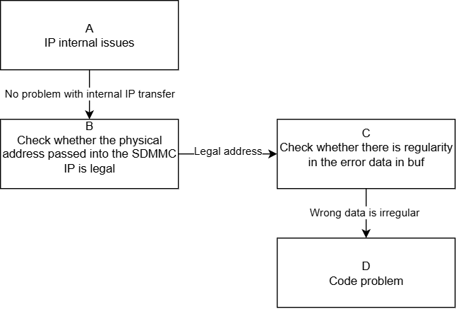
| Process | Method | Exit Conditions | Next Step | Information to be provided to SWRD | Related Reference FAQ |
|---|---|---|---|---|---|
| A | 1. The entire SD/SDIO protocol system can be abstracted into host, bus, and device according to the SPEC's SD/SDIO host modes. 2. Confirm that the padmux settings are correct and correspond to the current operating environment, and that the LA/oscilloscope displays waveforms and timing are normal, but the DMA_END event is not being received. 3. Combine with the host mode to rule out host CMD sending, bus communication, and device anomalies, and consider that there may be an issue with data transfer within the host-side IP. |
Exit Condition 1: 1. HW RD assists in interpreting the debug bus, and there is an anomaly within the IP, such as internal DMA transferring to MIU without ACK, etc. Exit Condition 2: 1. SDMMC IP is normal. |
Exit Condition 1: > Process ends Exit Condition 2: > B |
||
| B | 1. Refer to the specification document to confirm the valid DRAM address space for the SDMMC IP, and then confirm whether the physical address offset passed to the SDMMC IP is valid, i.e., the address composed of bank 1413/42 offset 0x3/0x4. | Exit Condition 1: 1. The physical address offset passed to the SDMMC IP exceeds the valid range. Exit Condition 2: 1. The physical address offset passed to the SDMMC IP is valid. |
Exit Condition 1: > Process ends Exit Condition 2: > C |
Exit Condition 1: 1. Use the standard address space allocation interface provided by the system to request a buffer. |
|
| C | 1. Construct a test pattern and confirm whether there is a regularity in the differences between the source pattern and the read/write obtained pattern. | Exit Condition 1: 1. The pattern errors are obviously regular, always occurring with the SDMMC driver cache-line size error. Exit Condition 2: 1. The pattern errors have no obvious regularity. |
Exit Condition 1: > Process ends Exit Condition 2: > D |
Exit Condition 1: 1. Confirm whether the SDMMC standard read/write interface is used; if not, further confirm whether the buffer is non-cache. 2. Assist RD in setting up a reproduction environment. |
|
| D | The SDMMC driver read/write process is normal, but there is an anomaly during the data transfer process within the IP. Consider the following points: 1. Whether the DMA burst length is set to 8, i.e., bank 1413/42 offset 0x2[5:4]. 2. Whether the read/write does not consider cache operations or is handled incorrectly. 3. Data synchronization issues caused by modern CPU out-of-order execution. |
Exit Condition 1: 1. DMA burst length is not set to the maximum. Exit Condition 2: 1. In the running environment with dcache-on, the buffer read/write did not perform invalid and flush operations, resulting in inconsistent data. Exit Condition 3: 1. Logic that requires synchronization calls did not perform memory barrier processing, leading to out-of-order execution. Exit Condition 4: 1. Other issues. |
Exit Condition 1: 1. Try manually setting the DMA burst to the maximum value of 8. Exit Condition 2: 1. Try performing flush operations during write operations and invalid operations after read operations. Exit Condition 3: Exit Condition 4: ==> Process ends |
Exit Condition 3: Exit Condition 4: 1. Confirm the status of the customer branch and the patches applied. 2. Assist RD in setting up a reproduction environment. |
4. Issues Related to Hot Swapping of SD Cards
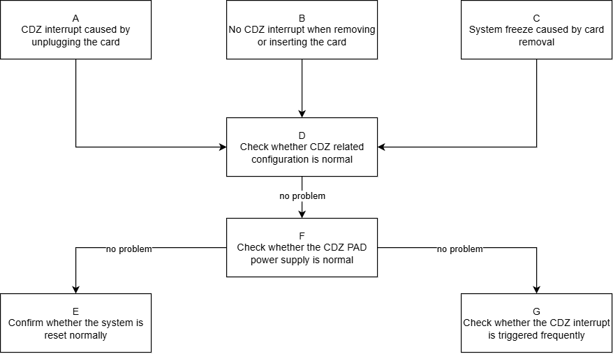
| Process | Method | Exit Conditions | Next Step | Information to be provided to SWRD | Related Reference FAQ |
|---|---|---|---|---|---|
| A | 1. The principle of CDZ interrupt trigger: The result after xor(src, polarity), i.e.: 1.1. When the level of CDZ src is 0, there will be an interrupt when the polarity level (0->1) occurs. 1.2. When the level of CDZ src is 1, there will be an interrupt when the polarity level (1->0) occurs. 2. After system wdt_rst or STR, there will be a CDZ interrupt that meets the trigger conditions. |
Exit Condition 1: 1. Confirm that the system is performing wdt_rst or STR operations. Exit Condition 2: 1. The system is running normally and has not executed wdt_rst or STR operations. |
Exit Condition 1: > E Exit Condition 2: > D |
||
| B | 1. First, check whether the CDZ-related configuration items are correctly enabling the CDZ interrupt. 2. If the configuration is fine, prioritize checking whether the SD card socket hardware is faulty and whether the CDZ pad power supply is normal. 3. Based on the CDZ trigger principle in A, check whether there are mismatches between src and polarity in the code. |
Exit Condition 1: 1. CDZ-related configurations are not correctly configured. Exit Condition 2: 1. The SD card socket has a fault causing abnormal CDZ pad power supply. Exit Condition 3: Code logic issue. |
Exit Condition 1: > D Exit Condition 2: > F Exit Condition 3: ==> Process ends |
Exit Condition 3: 1. Provide the accurate branch to RD for investigation. |
|
| C | 1. First, confirm whether the system anomaly is caused by the CDZ interrupt itself or by logic triggered after the insertion/removal action. 2. Check whether there are errors in the CDZ padmux configuration. |
Exit Condition 1: 1. CDZ-related configurations are not correctly configured. Exit Condition 2: 1. Confirm whether the CDZ interrupt itself is frequently triggered, causing system lag. Exit Condition 3: 1. Confirm whether the logic after inserting/removing the card causes the system to hang. |
Exit Condition 1: > D Exit Condition 2: > G Exit Condition 3: ==> Process ends |
Exit Condition 3: 1. Assist RD in setting up a reproduction environment. |
|
| D | 1. Confirm whether the CDZ padmux configuration for SD/SDIO corresponds to the development board, and whether the pad conflicts with other modes. Confirmation method: cd vim arch/arm/boot/dts/(chip name)_xxxx-padmux.dtsi 2. Confirm whether the CDZ-related configurations for SD/SDIO are correct: cd vim arch/arm/boot/dts/(chip name).dtsi Mainly check whether the 'fake-cdz' and 'rev-cdz' configuration items are correct; whether the 'cdz_slot0_irq' interrupt configuration is correct. |
Exit Condition 1: 1. CDZ padmux is not correctly configured; 2. CDZ-related configuration items are incorrectly configured. Exit Condition 2: 1. CDZ configuration is fine. |
Exit Condition 1: 1. Correctly configure according to padmux and actual operating environment. > Process ends Exit Condition 2: > F |
||
| E | 1. When the SD card is not inserted, after the system performs wdt_rst, it will meet the condition in A 1.2 and generate a CDZ interrupt. 2. When the SD card is not inserted, if the system performs STR, it will also meet the condition in A 1.2 and generate a CDZ interrupt during the resume phase. |
Exit Condition 1: 1. Confirm that the system has triggered a reset operation. Exit Condition 2: 1. The system is running normally and has not triggered any related reset operations. |
Exit Condition 1: 1. Seek assistance from the intr_ctrl owner to provide a solution to mask this non-application expected interrupt. Exit Condition 2: ==> Process ends |
Exit Condition 2: 1. Assist RD in setting up a reproduction environment. |
|
| F | 1. The CDZ pad is designed for hot swapping of SD cards, with the default state being a high level pulled up by an external 3.3V voltage. When the SD/SDIO card is inserted into the slot, the contact with the grounding plate changes to a low level. 2. The CDZ interrupt is edge-triggered bidirectionally, and the level state change of the CDZ pad caused by card insertion/removal will trigger the CDZ interrupt according to the principle in A. 3. Under correct CDZ-related configurations, the LA or oscilloscope can be used to observe whether there are fluctuations in the CDZ pad level. |
Exit Condition 1: 1. Observed fluctuations in the CDZ pad level are too large, reaching the CDZ trigger threshold; Exit Condition 2: 1. CDZ pad level is normal. |
Exit Condition 1: 1. Seek CAE assistance to investigate hardware. Exit Condition 2: ==> E/G |
||
| G | 1. When able to access the console: linux: cat /proc/interrupts |
grep cdz rtos: echo cli intrstat > /proc/dualos/rtos Check the number of CDZ interrupt triggers. 2. Use the tvtool tool to check the trigger situation of the CDZ interrupt corresponding to bank:0x1009. |
Exit Condition 1: 1. CDZ interrupt is triggered abnormally frequently; after umask irq, the system returns to normal. Exit Condition 2: 1. CDZ interrupt is normal, consistent with the number of insertions/removals. |
Exit Condition 1: > Process ends Exit Condition 2: > Process ends |
Exit Condition 1: Exit Condition 2: 1. Assist RD in setting up a reproduction environment |
5. Appendix
5.1 SDIO Device Initialization Process
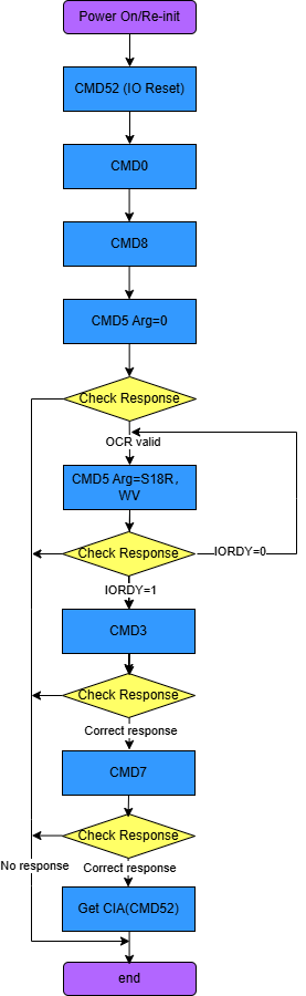


Regardless of the type of command, focus on the middle 32 bits of the request and response commands.
>>>sdio soft reset: cmd52 read/write CCCR register completed


The SDIO device will complete the reset enable operation by performing a cmd52 operation on the CCCR register at address 0x06, which is the I/O ABORT register's bit3. Generally,
the first two cmd52 commands will complete normally, but cmd52 often reports 0x8 no rsp err ("details can be found in Chapter 2"). The root cause is that the SDIO device
has not completed the power-on initialization procedure. To solve this problem, it is generally necessary to configure the 'pwr-off-delay' in the dtsi to delay it to over 150ms.
>>>device go idle: Effective for SDIO cards with storage



This is meaningful only for SDIO cards with storage; generally, the SDIO Wi-Fi card used is I/O only, and the actual soft reset is completed by the previous
cmd52.
>>>check sd card: Effective for SDIO cards with storage

This command is optional for the SDIO device, and theoretically, when using the SDIO device, the dtsi should configure 'no-sd' and 'no-emmc' to skip this step.
>>>cmd5: Get the operating voltage range supported by the SDIO card



During SDIO device initialization, cmd5 is the key; the previous cmd52/0/8 can report errors and continue down, because the SDIO device needs
a certain amount of time to power on to ready, but if the cmd5 command fails, it means that communication has really encountered an exception.
The first ARG:0x00000000 is mainly to obtain the voltage support range of the SDIO device.
The second ARG:0x00100000 sends the voltage supported by the host side and triggers the device initialization action.
The host will test the response of cmd5, polling to check whether ARG: bit31 is set to 1 (device ready).
>>>cmd3/cmd7: Host obtains the RCA address of the SDIO card and selects the card for operation based on the address



The host obtains the newly set RCA register of the SDIO card and selects the SDIO device for operation through cmd7 and the address returned by cmd3.
>>>Get CIA information: func0's CCCR/CIS information




After the host and device establish a link, it begins to obtain the basic information of the device. By accessing func0, it reads the CCCR device control register information. Each device
has func0, and both CCCR and each FBR have 256 bytes; the init flow will obtain some key information from them.
ARG:0x00000000 reads func0 (CCCR) at address 0x0, which is the CCCR/SDIO revision version information.
ARG:0x00001000 reads func0 (CCCR) at address 0x8, which is the Card Capability information, responding with: 0x00001013 indicating that the device supports
1. do CMD52 while data transfer
2. do multi-block xfers
3. interrupt during 4-bit CMD53.
ARG:0x00002400 reads func0 (CCCR) at address 0x12, which is the power control information, responding with: 0x00001001 indicating that the device supports the host
to perform power control.
ARG:0x00002600 reads func0 (CCCR) at address 0x13, which is the bus speed select information, responding with: 0x00001001 indicating that the device supports
High-Speed mode.




The CIS area provides more detailed information about the device.
ARG:0x00001200/0x00001400/0x00001600 three commands obtain func0 (CCCR) at addresses 0x9-0xb, i.e., the CIS pointer information, to access
CIS area information.
ARG:0x00200000/.../0x00202000 a series of commands are used to read information from the Common CIS area.
At this point, the host has obtained all the basic information related to func0 of the card.
>>>bus speed/bus width: Switch rate and bit width




ARG:0x00002600 reads func0 (CCCR) at address 0x13, which is the bus speed select information.
ARG:0x80002603 writes to func0 (CCCR) at address 0x13, enabling high-speed bus speed.
ARG:0x00000E00 reads func0 (CCCR) at address 0x7, which is the bus interface control information.
ARG:0x80000E02 writes to func0 (CCCR) at address 0x7, enabling 4-bit bus interface control.
At this point, the SDIO card will switch to a 4-bit 48MHz working environment.
>>>Get CIA information: func1's FBR/CIS information




The host accesses func0 to read the device control register information. It will then read the FBR/CIS information corresponding to each func from func1 to func7 based on the actual situation of the SDIO card.
The reading of FBR/CIS information is completely consistent with the reading of the above func0's CCCR/CIS general information, except that the func number in cmd52 changes to the corresponding func; generally, the SDIO card
will support func1 functionality.
ARG:0x00020000 reads func1 at address 0x100, which is the func1 SDUI function interface code information.
ARG:0x00021600 reads func1 at address 0x10b, which is the last item of func1's CIS pointer address.
The description here is omitted for the cmd52 between 0x100-0x10b.
ARG:0x00220000/.../0x00226000 a series of commands are used to read information from the func1 CIS area.
At this point, the core commands involved in the SDIO card initialization process are completed.
>>>SDIO card recognition successful

5.2 SD Card Initialization Process
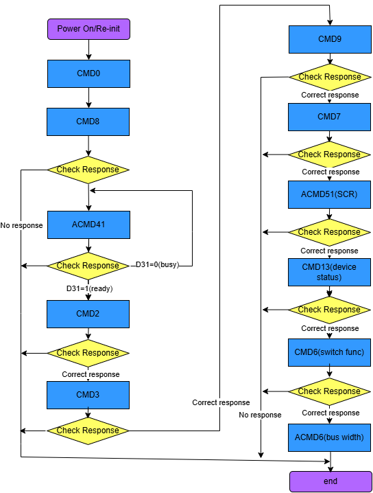
>>>sd go idle: cmd0 makes the card enter idle state

Initialization will power cycle the device, putting it into idle state.
>>>host sync support voltage: Let the card confirm whether it supports the voltage list provided by the host

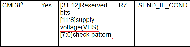
Obtain the voltage support range of the card, illustrated as a range of 2.7~3.6V.
>>>Get OCR information: The first time does not care about the card's state

During the probe, the first cmd41 is sent to obtain the card's OCR register information, regardless of the card's state.
>>>sd go idle again: cmd0 makes the card enter idle state
Adjust the host's support based on the card's OCR, power cycle the device, putting it into idle state.
>>>host sync updated support voltage: Let the card confirm whether it supports the voltage list provided by the host
>>>host sync capability set and confirm OCR information


Continuously polling the card's status, waiting for the device to be ready, testing whether ARG: bit31 is set to 1 (device ready).
>>>host obtains card CID information: Factory-set MID/OID and other identification information

>>>cmd3/cmd9/cmd7: Host obtains the RCA address of the SD card and retrieves CSD register information and selects the card for operation based on the address



>>>acmd51: Read SCR register information

The SCR register provides supplementary information to the CSD register, such as specification version information, etc.
>>>acmd13: Obtain device status information, transferring 512 bytes of register information via the data line

>>>host obtains check func information and executes switch func information


ARG:0x00FFFFF0, bit31 is 0, check switchable func information, mainly involving four groups: 1. access mode 2. command system 3. driver strength 4. power limit.
ARG:0x80FFFFF1, bit31 is 1, switch func operation, switching access mode to func1 for high-speed.
After this step, the SD clock will be adjusted to 48MHz.
>>>acmd6: Adjust device bus width

The set bus width operation adjusts the bus width to 4 bits.
After this step, because the card device is generated, it will match with the card driver to generate a block device node.
>>>SD card recognition successful

5.3 Common Error Waveforms and Logs for SD/SDIO
>>>cmd no rsp


The host has issued a cmd request and the clock is outputting normally, but no device response is received within 8T time.
The driver will print SD_STS:0x0F08 error code.
>>>cmd crc



After the host normally issues cmd17/18/24/25 write commands, there is a data response on the data line, and the last 5 bits of the write command dat0 are the CRC status confirmation identified by the device. The correct value is '00101', while the error value is '01011'.
The CRC for read commands is internally verified by the IP.
The driver will print SD_STS:0x0F01 (read CRC)/SD_STS:0x0F02 (write CRC) error codes.
>>>cmd timeout
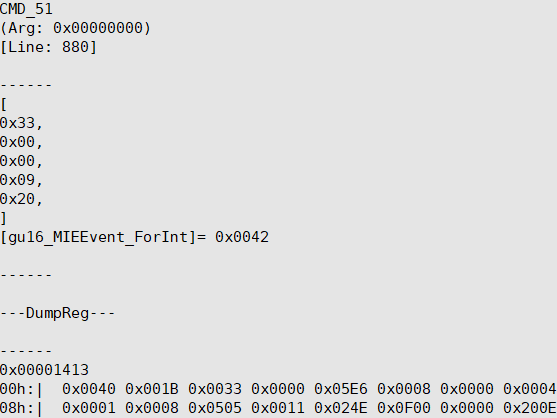

A cmd timeout is a judgment at the driver level, so the waveform is generally normal, mainly reflected in the driver's debug error log.
The driver will print (FAIL)= 0100 error code, indicating that the waiting time set by the driver has been reached, but the event has not been received. Refer to "2. SD/SDIO Communication Process Issues".
>>>cmd6 execution switch func error
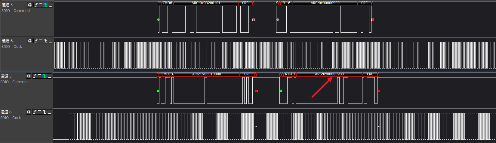
The cmd6 command is quite special; its response is of type r1b. If there is an error executing cmd6, the subsequent cmd13 response will provide feedback on the error status.
The image shows a switch error, with the cmd13 response status displaying '980', indicating a device switch error.
>>>Common timing issue 1: clk is turned off when cmd is issued
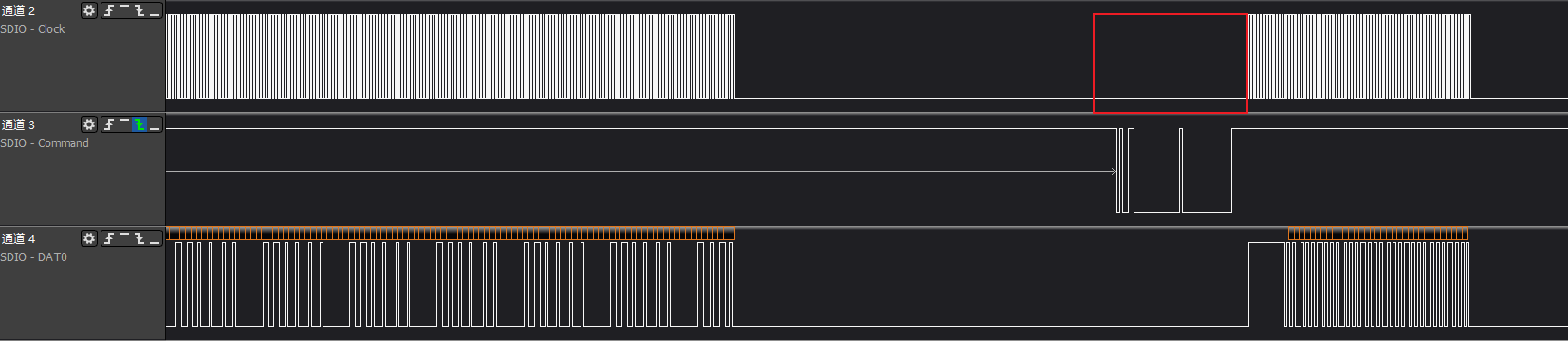
>>>Common timing issue 2: clk is abnormal when cmd is issued, causing cmd to not be recognized properly

>>>Common timing issue 3: External interference such as static electricity/high and low temperatures causes clk abnormalities
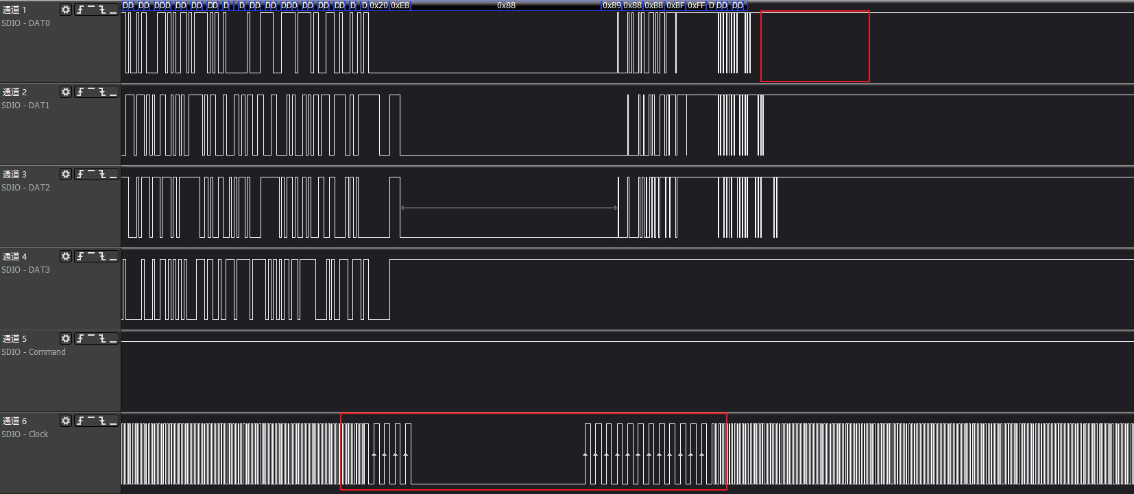
>>>Common timing issue 4: clk has almost no sampling setup time, easily leading to misjudgment
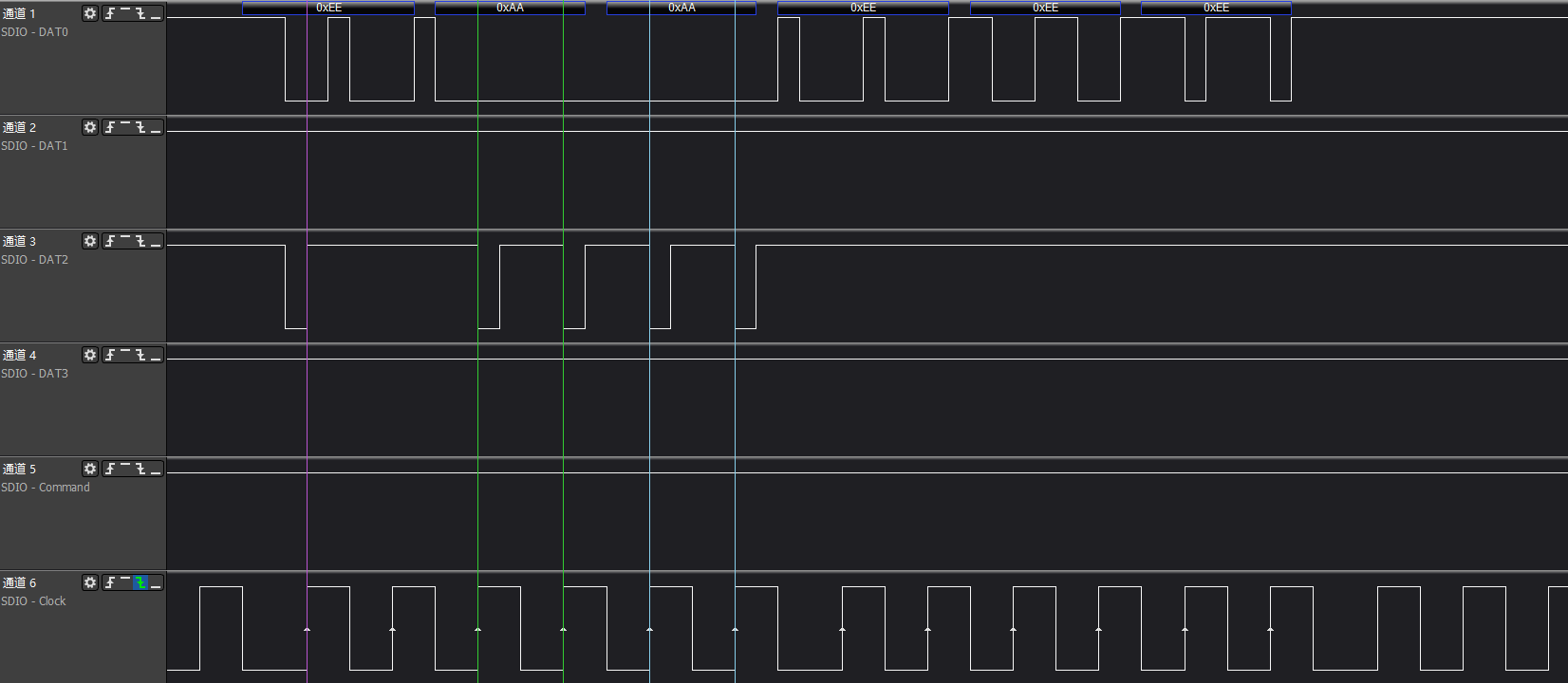
Timing issues are generally complex and require HW RD/CAE involvement to provide solutions. Common software methods generally include adjusting phase, improving drive capability, spreading frequency, etc.