SDMMC USER GUIDE
REVISION HISTORY
| Revision No. | Description |
Date |
|---|---|---|
| 1.0 | 04/15/2025 | |
| 2.0 | 01/04/2026 |
1. OVERVIEW
MMC under Kernel adopts the standard Linux framework and can use standard interfaces to drive MMC Device (eMMC card, SD card or SDIO device).
The MMC subsystem consists of the card layer, core layer and host layer. The card layer registers the entire MMC Device as an MMC Block Device, which can support the data request work of the upper layer; the core layer implements the initialization process and reading and writing work in the MMC/SD/SDIO protocol. The host layer can mobilize the hardware and communicate the cmd or data request passed down by the core layer with the eMMC/SD/SDIO card through the FCIE/SDIO Engine.
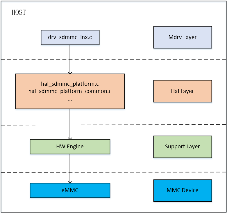
The overall framework of the SD host layer consists of three layers, namely the MDrv layer, the Hal layer, the Support layer, and the MMC device connected to the Support layer. The functions of each layer are as follows:
Drv layer:
The Drv layer mainly completes the host registration, improves the description of the mmc_host and mmc_host_ops structures, adds the host information to the core layer, and provides some additional encapsulation interfaces to set or obtain the status of the Engine and the card for the user layer, such as debug_get_sdmmc_clock, set_sdmmc_driving_control, etc. In addition, the Drv layer also completes the MIE and hot-swap interrupt registration to ensure the normal transmission of subsequent signals and the plug-in and plug-out detection of the card.
Hal layer:
The Hal layer directly sets registers and is closely related to the HW Engine. It mainly includes the hal_sdmmc_v5.c file that operates the Host Engine. The sending and receiving of commands and data is implemented in this file. The hal_sdmmc_platform_common.c file determines which group of pad pins the Host Engine connects to and performs operations such as pull-up and pull-down on it. The hal_sdmmc_intr.c file is related to interrupt processing, and the hal_sdmmc_timer.c file is related to time processing, etc.
Support layer:
This layer belongs to the hardware support layer, and the related final implementation of the driver requires hardware support.
MMC device:
MMC devices, such as SD/SDIO cards, are directly connected to the driver's hardware support and are the driver's final operation object.
2. KEYWORD DESCRIPTION
IP: Host Engine connected to SD/SDIO cards.
IP bank: Register address of Host Engine used by driver to access SD/SDIO cards.
SDSC: Standard capacity card, no larger than 2GB.
SDHC: High capacity card, larger than 2GB but no larger than 32GB.
SDXC: Extended capacity card, larger than 32GB.
3. FUNCTION DESCRIPTION
| Package | SD card | Bus bandwidth | Clock range | SD3.0 supported speed modes | SD2.0 supported speed modes | IP bank | Products |
|---|---|---|---|---|---|---|---|
| BGA14 | SD0 Card | 1, 4 | 300k-48M | Not supported | Default Speed, High Speed | FCIE: 0x1410 | pcupid |
| BGA14 | SD1 Card | 1, 4 | 300k-48M | Not supported | Default Speed, High Speed | SDIO: 0x1413 | pcupid |
| BGA | SD0 Card | 1, 4 | 300k ~ 200M | SDR50, SDR104, DDR50 | Default Speed, High Speed | 0x1413 | souffle |
| BGA | SD1 Card | 1, 4 | 300k ~ 100M | SDR50 | Default Speed, High Speed | 0x1416 | souffle |
| QFN | SD0 Card | 1, 4 | 300k ~ 200M | SDR50, SDR104, DDR50 | Default Speed, High Speed | 0x1413 | souffle |
| BGA | SD0 Card | 1, 4 | 300k ~ 48M | - | Default Speed, High Speed | 0x1413 (non-pm) | iford |
| BGA | WIFI Card | 1, 4 | 300k ~ 48M | - | Default Speed, High Speed | 0x42 (pm) | iford |
| FCCSP | SD0 Card | 1,4 | 300k-48M | SDR50,SDR104,DDR50 | Default Speed,High Speed | 0x1413 | ifackel |
| FCCSP | SD1 Card | 1,4 | 300k-48M | - | Default Speed,High Speed | 0x1413 | ifackel |
| BGA | SD0 Card | 1,4 | 300k-200M | SDR50,SDR104,DDR50 | Default Speed,High Speed | 0x1413 | jaguar1 |
| BGA | SD1 Card | 1,4 | 300k-100M | SDR50 | Default Speed,High Speed | 0x1416 | jaguar1 |
| QFN | SD Card | 1,4 | 300k-48M | - | Default Speed,High Speed | 0x1410 | ibopper |
| QFN | SD0 Card | 1,4 | 300k-48M | - | Default Speed,High Speed | 0x1413 | ifado |
| QFN | SD1 Card | 1,4 | 300k-48M | - | Default Speed,High Speed | 0x1410 | ifado |
| FCCSP | SD0 Card | 1,4 | 300k-48M | SDR50,SDR104,DDR50 | Default Speed,High Speed | 0x1413 | mhera |
Note: The pcupid BGA packaged board has 2 SD card slots, of which the default IP type of SD0 is FCIE, which does not support SDIO devices, the IP type of SD1 is SDIO, which supports SDIO devices, and the QFN package has only 1 SD card slot, the default IP type is SDIO, which supports SDIO devices.
Bus bandwidth setting:
SD supports configuring 1-1bit mode/4-4bit mode two bus bandwidths, and the default mode is 4bit mode. The SDIO card needs to set the bandwidth to 1bit mode, which can be set by setting the sdio-use-1bit parameter in the device tree.
Clock setting:
The clock ranges that can be set for different rate modes are shown in the figure below. The maximum clock can be set by modifying the max-frequency parameter in the device tree.
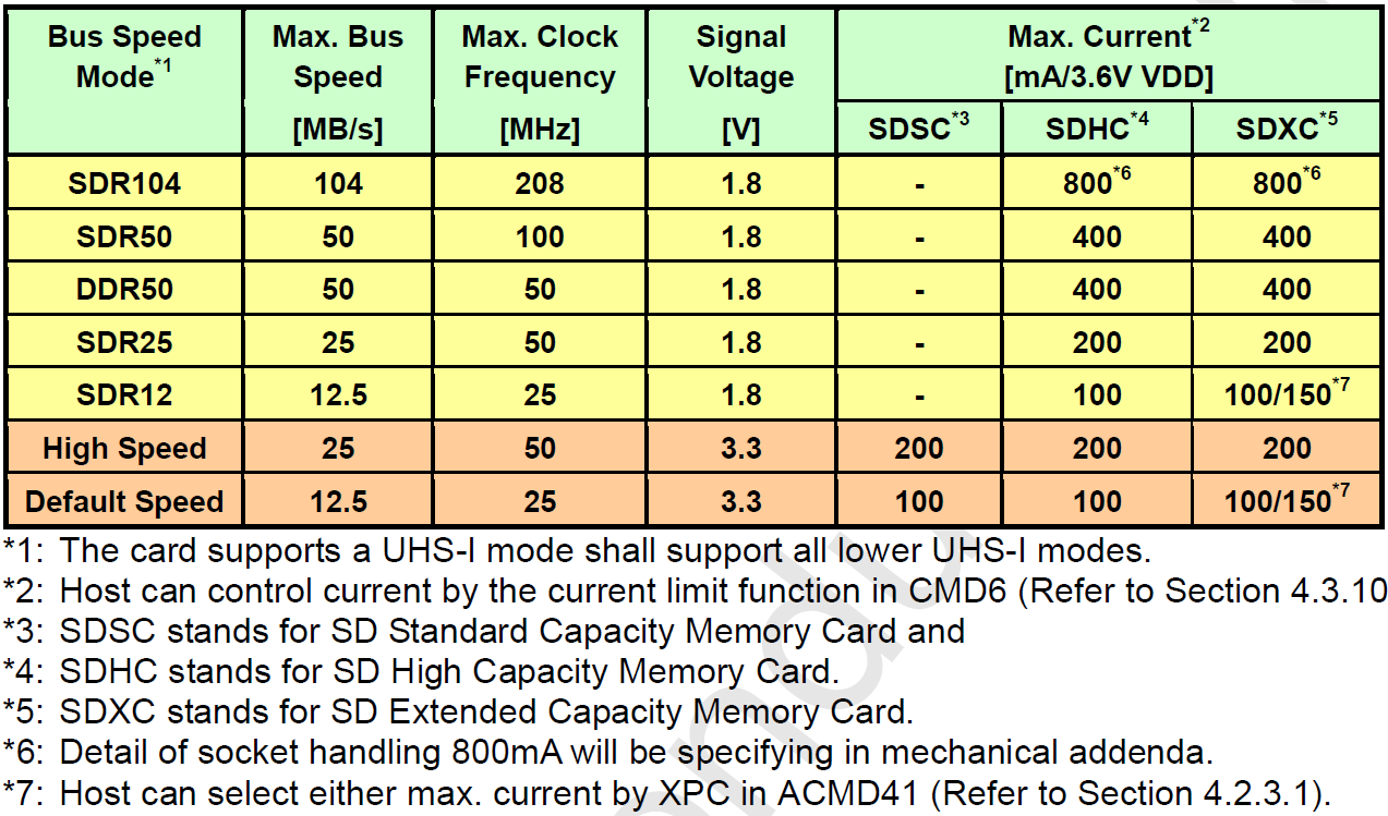
Configuring different bus bandwidths and clock frequencies will affect the data transfer speed. SD3.0 supports the use of SDR50, SDR104 and DDR50 speed modes. If you want to use them, you can configure sd-uhs-sdr50/sd-uhs-sdr104/sd-uhs-ddr50 in the corresponding slots in the device tree.
When using High Speed mode, the clock frequency and theoretical speed supported by the hardware refer to the following table(implies x4 bus width).
| No | Clock frequency(Hz) | Transfer rate(MB/s) |
|---|---|---|
| 0 | 300000 | 1.5 |
| 1 | 12000000 | 6 |
| 2 | 20000000 | 10 |
| 3 | 32000000 | 16 |
| 4 | 36000000 | 18 |
| 5 | 40000000 | 20 |
| 6 | 43200000 | 21.6 |
| 7 | 48000000 | 24 |
When configuring the SDR50, DDR50, and SDR104 speed modes, refer to the following table for the theoretical speeds(implies x4 bus width).
| No | Clock frequency(Hz) | Transfer rate(MB/s) |
|---|---|---|
| 0 | 12000000-100000000 (SDR50) | 6-50 |
| 1 | 12000000-50000000 (DDR50) | 12-50 |
| 2 | 12000000-208000000 (SDR104) | 6-104 |
Note that the actual read and write speed is affected by factors such as cmd transmission consumption and mmc device performance during the read and write process, and cannot reach the theoretical speed. To test the performance, it is recommended to use the fio tool to read and write large files for testing.
Speed Mode:
(1) Check the SD card speed mode.
cat /sys/kernel/debug/mmc1/ios
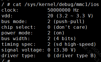
Figure 3-2: Sdmmc-12
(2) Set the SD card speed mode.
The SD card speed mode can be directly configured in the dtsi file.
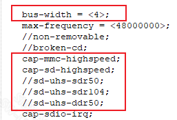
Figure 3-3: Sdmmc-13
4. HARDWARE CONNECTION INTRODUCTION
4.1. mhera
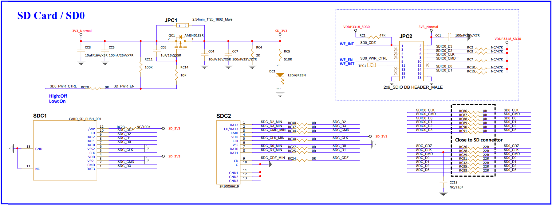
The software padmux settings corresponding to the hardware connection are as follows:
1.    padmux {
2.        compatible = "sgs-padmux";
3.        schematic =
4.            // SDMMC0
5.            <PAD_SD0_D1              PINMUX_FOR_SD0_MODE_1           MDRV_PUSE_SDIO0_D1>,
6.            <PAD_SD0_D0              PINMUX_FOR_SD0_MODE_1           MDRV_PUSE_SDIO0_D0>,
7.            <PAD_SD0_CLK             PINMUX_FOR_SD0_MODE_1           MDRV_PUSE_SDIO0_CLK>,
8.            <PAD_SD0_CMD             PINMUX_FOR_SD0_MODE_1           MDRV_PUSE_SDIO0_CMD>,
9.            <PAD_SD0_D3              PINMUX_FOR_SD0_MODE_1           MDRV_PUSE_SDIO0_D3>,
10.           <PAD_SD0_D2              PINMUX_FOR_SD0_MODE_1           MDRV_PUSE_SDIO0_D2>,
11.           <PAD_SD0_GPIO0           PINMUX_FOR_GPIO_MODE            MDRV_PUSE_SDIO0_PWR>,
12.           <PAD_SD0_CDZ             PINMUX_FOR_SD0_CDZ_MODE_1       MDRV_PUSE_SDIO0_CDZ>,
13.    };
5. UBOOT USAGE INTRODUCTION
5.1. Uboot Config Configuration
1. make menuconfig
2. # sgs drivers -->
3. # -*-   SGS SD/MMC Card Interface Support
4. #    Sgs SDMMC DDR Mode (sdr/ddr Mode)  --->)  --->
5. #    Sgs SDMMC RECEIVE RESPONSE Mode (polling Mode)  --->)  --->
6. # [ ]     Support SD30
7. # [ ]     Support EMMC50
8. # [ ]     Support SDMMC Command
9. # [ ]     Support SDMMC AT/SMOKE test
10.# [ ]     SELECT EMMC
11.# [ ]     enable fcie ip drive sd atop
12.# -*-   Sgs mmc host
13.# [ ]     Support SDIO driver
The directory where the SDMMC driver is located under boot is drivers/sgs_common/sdmmc. The compilation option SGS_MMC_HOST needs to be enabled. The opening method is as above.
| Function | Describe | Remark |
|---|---|---|
| SELECT EMMC | FCIE IP is configured as EMMC function | Only used by pcupid/iford/jaguar1 products, need to be enabled when using EMMC |
| Support SDIO driver | Configure the driver to support SDIO card recognition | Enable as needed |
| enable fcie ip drive sd atop | FCIE IP chooses to use SDPLL as the clock source | Only used by ifackel products, FCIE IP needs to be enabled when running SD3.0 |
5.2. DTS Parameter Configuration Description
You can set the basic parameters of the host layer driver by configuring the sgs_mmc0 item in dtsi. The parameters of dtsi are shown as follows:
        sgs_mmc0: sgs_mmc0 {
            compatible = "sgs-mmc";

            bus-width = <4>;
            max-frequency = <48000000>;
            cap-sd-highspeed = <1>;
            ip-order = <2>;
            pad-order = <1>;
            pwr-on-delay = <10>;
            pwr-off-delay = <50>;
            fake-cdz = <0>;
            rev-cdz = <0>;
            pwr-pad = <PAD_GPIOE_07>;
            cdz-pad = <PAD_GPIOE_06>;
            clk-driving = <1>;
            cmd-driving = <1>;
            data-driving = <1>;
            en-clk-phase = <0>;
            rx-clk-phase = <0>;
            tx-clk-phase = <0>;
            status = "okay";
        };
The definitions are as follows:
| Parameter | Definition | Remark |
|---|---|---|
| bus-width | Configure the buswidth of the card slot | 4 - 4bit mode |
| max-frequency | Configure the maximum clock frequency supported by the corresponding card slot | Uboot supports 48MHz |
| ip-order | Configure the IP number of the corresponding card slot | Modification prohibited |
| pad-order | Specify which pad group the card is connected to | Public version software is not used and does not need to be modified |
| pwr-on-delay | Configure the power-on delay time of each card slot in ms | SDIO devices generally need to configure a delay time so that the SDIO device can load the firmware and the state is ready. The specific time is subject to the recommendations of the SDIO device manufacturer(EMMC/SD device nodes do not need to be modified) |
| pwr-off-delay | Configure the power-off delay time of each card slot in ms | Configure the power-on delay time of each card slot in ms |
| fake-cdz | Configure whether to ignore Card detect. Setting it to 1 means that the slot is assumed to have a card connected by default | For devices fixed on the board, such as some SDIO devices, the slot corresponding item should be configured as 1 |
| rev-cdz | This parameter can be used to configure whether to reverse the Card detect condition of the current Board | By default, the card is detected at a low level. If the hardware design shows that the CDZ level is high after the card is inserted, configure this item to 1. |
| clk-driving | Configure the driving capability of the clock pad pin of the corresponding card slot | This item generally does not need to be modified. If you encounter communication signal quality problems, you can adjust this item based on the waveform. |
| cmd-driving | Configure the driving capability of the command pad pin of the corresponding card slot | This item generally does not need to be modified. If you encounter communication signal quality problems, you can adjust this item based on the waveform. |
| data-driving | Configure the driving capability of the data[3:0] pad pin of the corresponding card slot | This item generally does not need to be modified. If you encounter communication signal quality problems, you can adjust this item based on the waveform. |
| en-clk_phase | Configure whether to enable clock phase tuning for the corresponding card slot | When CRC problems occur in device read/write communications, they can be solved by changing the sampling points of rx and tx. |
| rx-clk_phase | Configure the clock tx phase of the corresponding card slot | Gear: 0-3, this parameter is valid only when en-clk_phase is set to 1, each gear phase interval is 90° |
| tx-clk_phase | Configure the clock rx phase of the corresponding card slot | Gear: 0-3, this parameter is valid only when en-clk_phase is set to 1, Each gear phase interval is 90° |
| non-removable | Configure whether the device is non-removable | No modification is required, EMMC devices need to configure this item |
5.3. Uboot Cmd Parameter Description
(1) fatls
Format:
Description: Read all the file contents in a directory in the nth partition of the nth device under a certain interface.
Interface: Both SD cards and eMMC cards belong to MMC devices.
Dev: Device number, according to the ip number, the default is 0.
Part: Corresponds to the partition number under the mmc part command.
Directory: Directory, use the absolute path.
Example: Print the contents of the root directory in the first partition of SD.
(2) fatload
Format:
Description: Read data of a specific size from a file in the nth partition of the nth device under a certain interface to the ddr at the specified address.
Addr: Target memory address, ddr address, use real physical address.
Filename: File name to be loaded, use the absolute path file name.
Bytes: Data size to be loaded, in bytes, hexadecimal number, if 0, read the entire file.
Pos: Offset in the target file. For example, if the target file data is "123456", if pos is 1, read from position '1' when loading the file.
Example: Read 512 bytes of the demo.sh file in the root directory of the first partition of SD to 0x21000000 of ddr.
(3) fatwrite
Format:
Description: Read a specific size of data <bytes> from the ddr at the specified address and write it to a file in the nth partition of the nth device under a certain interface.
Addr: Source memory address, ddr address, use the real physical address.
Filename: The file name to be written, use the absolute path file name.
Bytes: The data size to be written, in bytes, hexadecimal.
Example: Read 512 bytes from ddr 0x21000000 and write it to the demo.sh file in the root directory of the first partition of SD.
(4) fatinfo
Format:
Description: Display the nth partition information of the nth device under a certain interface.
(5) fatsize
Format:
Description: Find the file of the nth partition of the nth device under a certain interface and calculate the file size.
5.4. Uboot Cmd Use Case
(1) fdisk
Fdisk is used to manage Linux disks, perform partitioning and formatting operations.
fdisk -p displays partition information.

Figure 5-1: Sdmmc-5
(2) fdisk -d 0: Delete all partitions of device 0
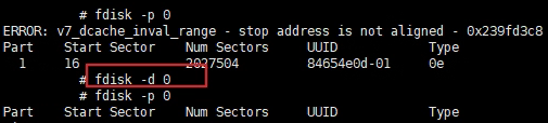
Figure 5-2: Sdmmc-6
(3) fdisk -c 0 0x32000: Create partition 1 and specify the partition size as 0x32000 blocks

Figure 5-3: Sdmmc-7
(4) fdisk -c 0 0x4800: Create partition 2 and specify the partition size as 0x4800 blocks

Figure 5-4: Sdmmc-8
(5) fdisk -c 0 0x64000: Create partition 3 and specify the partition size as 0x64000 blocks
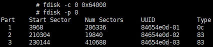
Figure 5-5: Sdmmc-9
(6) fdisk -c 0 0x96000: Create partition 5 and specify the partition size as 0x96000 blocks. Partition 4 is the extended partition mbr and needs to be skipped
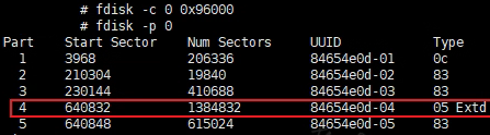
Figure 5-6: Sdmmc-10
(7) fdisk -c 0 0x400000: Create partition 6 and specify the partition size as 0x400000 blocks
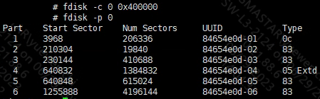
Figure 5-7: Sdmmc-11
6. KERNEL USAGE INTRODUCTION
6.1. Kernel Config Configuration
1. Associated Driver Module
The Card layer (mmc_block.ko) and the Core layer (mmc_host.ko) use the Linux standard code, and the Host layer (kdrv_sdmmc.ko) is maintained by sgs. In menuconfig, you can choose to compile them into the kernel or compile them into ko.
2. Enable the Corresponding Driver Module
1. make menuconfig
2. # Device Drivers -->
3. #    <*> MMC/SD/SDIO card support -->                   (mmc_core.ko)
4. #        <*> MMC block device driver                    (mmc_block.ko)
5. #    [*] SGS SoC platform drivers -->
6. #         <M>   SGS SD/MMC Card Interface Support       (kdrv_sdmmc.ko)
7. #         Sgs SDMMC DDR Mode (sdr/ddr Mode)  --->)  --->
8. #         Sgs SDMMC RECEIVE RESPONSE Mode (interrupt Mode)  --->)  --->
9. #         [*]     Support SD30
10.#         [*]     Support EMMC50
11.#         [ ]     Support SDMMC Command
12.#         [ ]     Support SDMMC AT/SMOKE test
13.#         [ ]     SELECT EMMC
14.#         [ ]     enable fcie ip drive sd atop
15.#         [ ]     Support SDMMC debuginfo
16.#         [ ]   Sgs mmc host
| Function | Describe | Remark |
|---|---|---|
| Support SD30 | Configure the driver to support SD3.0 protocol | Only ifackel, jaguar1 products support this function. |
| Support EMMC50 | Configure the driver to support EMMC5.0 protocol | Only pcupid, ifackel, jaguar1 products support this function. |
| Support SDMMC Command | After it is enabled, some debugfs debugging interfaces will be provided additionally | Enable as needed |
| Support SDMMC UT verify | Driver function debugging switch | No need to turn on |
| Support SDMMC AT/SMOKE test | Automated test switch | No need to turn on |
| SELECT EMMC | FCIE IP is configured as EMMC function | Only used by pcupid products, need to be enabled when using EMMC |
| enable fcie ip drive sd atop | FCIE IP chooses to use SDPLL as the clock source | Only used by ifackel products, FCIE IP needs to be enabled when running SD3.0 |
| Support SDMMC debuginfo | Enable debugfs debugging information node | Enable during debugging |
6.2. DTS Configuration Parameter Description
You can set the basic parameters of the host layer driver by configuring the sgs_sdmmc1 item in dtsi. The parameters of dtsi are shown as follows:
sgs_sdmmc1: sgs_sdmmc1 {
            compatible = "sgs,sdmmc";

            bus-width = <4>;
            max-frequency = <48000000>;
            //non-removable;
            //broken-cd;
            //cap-sd-highspeed;
            //sd-uhs-sdr50;
            //sd-uhs-sdr104;
            //sd-uhs-ddr50;
            //cap-sdio-irq;
            //no-sdio;
            //no-sd;
            //no-mmc;
            reg = <0x0 0x1F282600 0x0 0x200>;//1413
            pll-reg = <0x1F283200 0x200>;//1419
            cifd-reg = <0x1F282800 0x200>;//1414
            pwr-save-reg = <0x1F282A00 0x200>;//1415
            ip-order = /bits/ 8 <0>;
            pad-order = /bits/ 8 <0>;
            trans-mode = /bits/ 8 <1>;
            cifd-mcg-off = /bits/ 8 <0>; // mcg on/off in cifd
            ssc-switch =  /bits/ 8 <0>;
            fake-cdz = /bits/ 8 <0>;
            rev-cdz = /bits/ 8 <0>;
            cdz-pad = <PAD_GPIOA_06>;
            pwr-pad = <PAD_GPIOA_07>;
            pwr-on-delay = <1000>;
            pwr-off-delay = <300>;
            dev-ctrl-delay = <1>;
            en-pwr-high-valid = <0>;
            en-ctrl-high-valid = <0>;
            sdio-use-1bit = /bits/ 8 <0>;
            clk-driving = <1>;
            cmd-driving = <1>;
            data-driving = <1>;
            en-clk-phase = /bits/ 8 <0>; //0/1
            rx-clk-phase = <0>; //0-3
            tx-clk-phase = <0>; //0-3
            en-eight-phase = /bits/ 8 <0>; //0/1
            rx-eight-phase = /bits/ 8 <0>; //0/1
            tx-clk-phase = <0>; //0-3
            en-eight-phase = /bits/ 8 <0>; //0/1
            rx-eight-phase = /bits/ 8 <0>; //0/1
            tx-eight-phase = /bits/ 8 <0>; //0/1
            interrupts = <GIC_SPI INT_IRQ_SD IRQ_TYPE_LEVEL_HIGH>,
                        <GIC_SPI INT_FIQ_SD_CDZ_IN_0 IRQ_TYPE_LEVEL_HIGH>;
            interrupt-names = "mie0_irq", "cdz_slot0_irq";
            clocks = <&CLK_sd>;
            clock-names = "clk_sdmmc0";
            status = "ok";
        };
As shown in the figure above, the definitions of the SD/SDIO device tree configuration nodes are:
| Parameter | Definition | Remark |
|---|---|---|
| bus-width | Configure the buswidth of the corresponding card slot | 4 - 4bit mode |
| max-frequency | Configure the maximum clock frequency supported by the corresponding card slot | |
| non-removable | Configure whether the device is non-removable. Setting 1 means that the device is non-removable by default | eMMC/SDIO devices are generally set to non-removable attributes |
| broken-cd | Configure whether to use cdz interrupt | This property is configured for non-pluggable devices. |
| cap-mmc-highspeed | Configure whether the device supports mmc highspeed bus speed mode | Enable mmc highspeed mode by default |
| cap-sd-highspeed | Configure whether the device supports sd highspeed bus speed mode | Enable sd highspeed mode by default |
| sd-uhs-sdr50 | Configure whether to enable the sdr50 bus speed mode | pcupid does not support |
| sd-uhs-sdr104 | Configure whether to enable the sdr104 bus speed mode | pcupid does not support |
| sd-uhs-ddr50 | Configure whether to enable the ddr bus speed mode | pcupid does not support |
| cap-sdio-irq | Configure whether to enable sdio interrupt mode | Used by SDIO devices, comment out no-sdio when using SDIO devices |
| no-mmc | Configure the device does not support eMMC protocol | SD/SDIO devices do not support eMMC protocol |
| no-sd | Configure the device does not support sd protocol | EMMC/SDIO devices do not support sd protocol |
| no-sdio | Configure the device does not support sdio protocol | EMMC/SD devices do not support sdio protocol |
| reg | Configure SD/SDIO Host Engine Bank address | Modification prohibited |
| pll-reg | Configure SD/SDIO Host Engine PLL Bank address | Modification prohibited |
| cifd-reg | Configure SD/SDIO Host Engine CIFD Bank address | Modification prohibited |
| pwr-save-reg | Configure SD/SDIO Host Engine PSM Bank address | Modification prohibited |
| ip-order | Configure the IP number of the corresponding card slot | Modification prohibited |
| pad-order | Configure the padmux mode number of the corresponding card slot | Public version software is not used and does not need to be modified |
| trans-mode | Configure the data transmission mode of the corresponding card slot | No modification required |
| fake-cdz | Configure whether the corresponding card slot ignores Card Detect | Non-pluggable devices are configured as 1 |
| rev-cdz | Configure CDZ detection direction | By default, the card is detected at a low level. If the hardware design shows that the CDZ level is high after the card is inserted, configure this item to 1. |
| pwr-on-delay | Configure the power-on delay time of each card slot in ms | SDIO devices generally need to configure a delay time so that the SDIO device can load the firmware and the state is ready. The specific time is subject to the recommendations of the SDIO device manufacturer(EMMC/SD device nodes do not need to be modified) |
| pwr-off-delay | Configure the power-off delay time of each card slot in ms | Configure the power-on delay time of each card slot in ms |
| dev-ctrl-delay | Configure the delay time before and after the polarity reversal of the Ctrl pin, in milliseconds. | If the device requires an additional enable pin to control the chip, configure it according to the control timing recommended by the device manufacturer. |
| en-pwr-high-valid | Configure the effective polarity of the power output | 0 indicates low-level enable, 1 indicates high-level enable. |
| en-ctrl-high-valid | Configure Ctrl pin output polarity | 0 indicates low-level enable, 1 indicates high-level enable. |
| sdio-use-1bit | Configure the buswidth of the corresponding card slot to 1bit mode | Both SD/SDIO devices can be set |
| support-cmd23 | Configure whether to support the preset transmission block number function | eMMC device use |
| clk-driving | Configure the driving of the clock line of the corresponding card slot | This item generally does not need to be modified. If you encounter communication signal quality problems, you can adjust this item based on the waveform. |
| cmd-driving | Configure the driving of the cmd line of the corresponding card slot | This item generally does not need to be modified. If you encounter communication signal quality problems, you can adjust this item based on the waveform. |
| data-driving | Configure the driving of the data line of the corresponding card slot | This item generally does not need to be modified. If you encounter communication signal quality problems, you can adjust this item based on the waveform. |
| en-clk-phase | Configure whether to enable clock phase tuning for the corresponding card slot | 0 - Disable / 1 - Enable |
| rx-clk-phase | Configure the clock rx four-phase of the corresponding card slot | Gear: 0-3, en-clk-phase is set to 1 to make this parameter effective |
| tx-clk-phase | Configure the clock tx four-phase of the corresponding card slot | Gear: 0-3, en-clk-phase is set to 1 to make this parameter effective |
| en-eight-phase | Configure whether the corresponding card slot enables clock 8 phase tuning | 0 - Disable / 1 - Enable |
| rx-eight-phase | Configure the clock rx eight-phase of the corresponding card slot | For details, see clk phase usage instructions. |
| tx-eight-phase | Configure the clock tx eight-phase of the corresponding card slot | For details, see clk phase usage instructions. |
| interrupts | Configure interrupt information | Modification prohibited |
| interrupt-names | Configure interrupt names | Modification prohibited |
| clocks | Configure the eMMC Host Engine clock source | Modification prohibited |
| clock-names | Configure the clock source name | Modification prohibited |
clk phase instructions:
When using the four-phase mode, en-clk-phase needs to be set to 1, and then set the values of rx-clk-phase and tx-clk-phase according to the phase to be set, with a phase interval of 90°. When using the eight-phase mode, en-clk-phase and en-eight-phase need to be set to 1, and then set the values of rx-clk-phase, tx-clk-phase, rx-eight-phase and tx-eight-phase according to the phase to be set, with a phase interval of 45°.
Phase values corresponding to different phases
-
four-phase mode
phase rx-clk-phase tx-clk-phase 0° 0 0 90° 1 1 180° 2 2 270° 3 3 -
eight-phase mode
phase rx-clk-phase rx-eight-phase tx-clk-phase tx-eight-phase 0° 0 0 0 0 45° 1 0 1 0 90° 2 0 2 0 135° 3 0 3 0 180° 0 1 0 1 225° 1 1 1 1 270° 2 1 2 1 315° 3 1 3 1 -
Note 1: The default setting of hardware tx phase is 180°, so when the phase is set to 180°, the waveform of tx will be the same as when the phase is not turned on. When it is set to 0°, the phase will be 180° different from when the phase is not turned on.
-
Note 2: rx and tx can be set separately.
-
Note 3: When using the four-phase mode, the clock will be divided into four, and when using the eight-phase mode, the clock will be divided into eight. When the software setting has been turned on the phase function, the clock frequency will automatically be set to correspond to X4 and X8. When using the four-phase mode, when the clock frequency is 48M, the software sets 48M X 4, which is 192M, but the hardware is limited to no 192M clock source, and the 108M clock source (four-division is 27M) will be used downward, so it will be downgraded. Therefore, when using a 48M clock, it is recommended to use the eight-phase mode (48M X 8 = 384M). After setting the phase, the clock frequency output is still 48M. When using other clock frequencies, you need to choose which mode to use according to the previous description.
-
Note 4: When the spread spectrum is turned on, the clock source will select spi_synth_pll. The clock frequency generated by spi_synth_pll is continuous and the setting range is 12M-266M. Therefore, if you need to output a 48M clock, you need to select the four-phase mode (the maximum clock output of the eight-phase is 266M/8 = 33M). In addition, since spi_synth_pll is also the clock source used by flash, when flash and spread spectrum need to be used at the same time, It is recommended to switch the flash memory to another clock source.
SD card configuration example in dts file
        sgs_sdmmc1: sgs_sdmmc1 {
            //non-removable;
            //broken-cd;
            cap-sd-highspeed;
            //cap-sdio-irq;
            no-sdio;
            //no-sd;
            no-mmc;
            fake-cdz = /bits/ 8 <0>;
        };
SDIO card configuration example in dts file
        sgs_sdmmc1: sgs_sdmmc1 {
            //non-removable;
            //broken-cd;
            cap-sd-highspeed;
            cap-sdio-irq;
            //no-sdio;
            no-sd;
            no-mmc;
            fake-cdz = /bits/ 8 <0>;
        };
Control the timing of power pin and dev ctrl pin in the driver
The device will be powered off only when it is reinitialized.

6.3. Sample Code
None.
6.4. Module Usage Introduction
After the Linux system starts, the SD/SDIO driver is loaded normally, and the SD/SDIO Card is recognized, the SD Card will create the corresponding block device node /dev/mmcblk*. Use fdisk, mkfs, mount, and dd tools to apply for partitions, format partitions, mount partitions, and read and write mounted partitions for MMC devices.
In addition, the driver provides sysfs for debugging. For example, you can enter the /sys/class/mmc_host/mmc1/device/ directory to perform operations:
1.  cd /sys/class/mmc_host/mmc0/device/
2.
3.  # View SD/SDIO Host clock frequencey
4.  cat debug_get_sdmmc_clock
5.
6.  # View the last communication status between SD/SDIO Host and Device
7.  cat debug_get_sdmmc_status
6.
7.  # Set the driving capability of SD/SDIO pin
8.  echo [slotIndex] [signalLine] [drvLevel] > set_sdmmc_driving_control
9.  echo [slotIndex]  [drvLevel] > set_sdmmc_driving_control
10. echo [signalLine] [drvLevel] > set_sdmmc_driving_control
11. echo [drvLevel] > set_sdmmc_driving_control
12. #[slotIndex]: 0-1
13. #[signalLine]: "clk"/"cmd"/"data"/"all"
14. #[drvLevel]: 0-3
15.
16.  # Rescan SD/SDIO card
17.  echo [slot] > sdmmc_rescan
18.
19. # Set the spread spectrum parameters
20. ssc set param usage:
21. 1. echo [slotIndex] [modulation] [deviation] > sdmmc_setssc
22.    operation [slotIndex]   is slot number:0-2.
23.    operation [modulation]  value is between [20, 40], origin default is 20
24.    operation [deviation]   value is between [1000, 3001], origin default is 3001
25.    e.g. echo 0 20 1001 > sdmmc_setssc
26. 2. echo [slotIndex] [disable ssc] > sdmmc_setssc
27.    disable: e.g. echo 0 0 > sdmmc_setssc
28.    enable: e.g. echo 0 1 > sdmmc_setssc
29.
30. # Set the clock phase
31. set phase param usage:\n");
32. 1. echo [mode] [tx-clk-phase] [rx-clk-phase] [tx-eight-phase] [rx-eight-phase] > sdmmc_clk_phase
33.     operation [mode]               is phase mode:4 or 8
34.     operation [tx/rx-clk-phase]    value is between [0, 3]
35.     operation [tx/rx-eight-phase]  value is between [0, 1]
36.     e.g. Four-phase mode(180°):
37.         echo 4 2 2 > sdmmc_clk_phase
38.     e.g. Eight-phase mode(180°):
39.         echo 8 0 0 1 1 > sdmmc_clk_phase
40. 2. echo [enable/disable clk phase] > sdmmc_clk_phase
41.     disable: e.g. echo 0 > sdmmc_clk_phase
42.     enable: e.g. echo [4/8] > sdmmc_clk_phase
Spread spectrum parameter usage instructions:
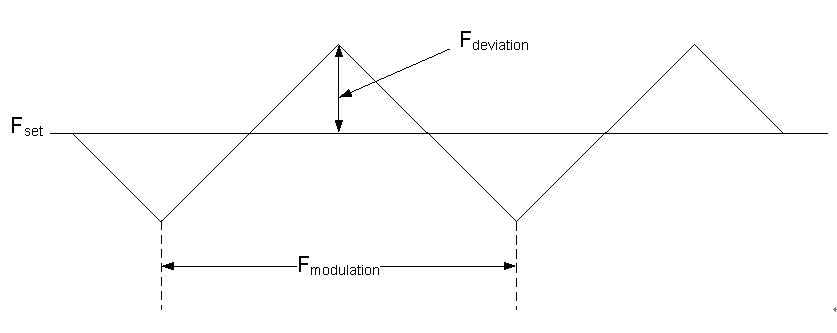
There are 3 parameters which may affect the modulation rate of SSC function: SET, SPAN and STEP.
-
PLL_SET = (MPLL*524288)/(SYN_CLK)
SPAN (14 bits)
STEP (12 bits)
SPAN = (MPLL * 131072) / (PLL_SET * Fmodulation)
STEP = (PLL_SET * Rdeviation) / SPAN
Fmodulation is the modulation frequency of SSC, it’s range is (20KHz ~ 40KHz)
Rdeviation is the deviation of SSC.(the max range is +-3 %)
Example:
Set the spread spectrum modulation frequency to 40KHz and the deviation to +-1%
echo 0 40 1000 > sdmmc_setssc
-
SYN_CLK = 75Mhz
ref_clk = 432Mhz
Modulation is 40KHz
Deviation is 1%
SET = ( 432MHz * 524288) / (75MHz ) = 3019899 = 0x2E147B
SPAN = (432MHz * 131072)/ ( 3019899 * 40KHz) = 468 = 0x1D4
STEP = (3019899 * 1%) /468 = 64 = 0x40
7. API REFERENCE
None.
8. DEBUG & FAQ
The driver provides a debug node for obtaining debugging information. You can find the debug node after entering the /sys/devices/virtual/sgs/mmcx directory. The usage of the debug node is introduced below.
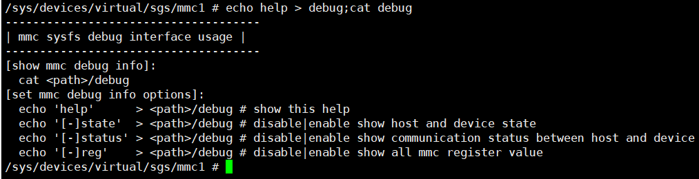
Type echo help > debug and then cat debug to check the usage of debug.
8.1. Query device node status
echo state > debug;cat debug
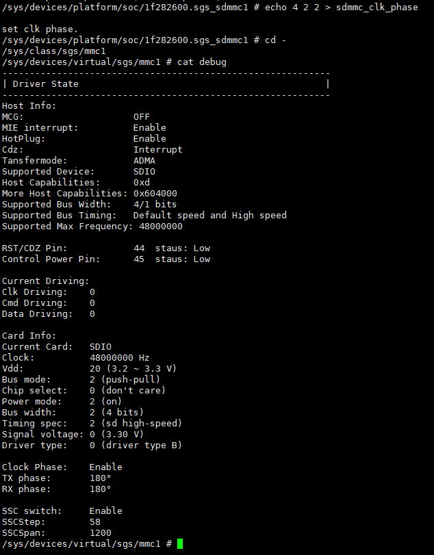
| attribute | Definition |
|---|---|
| MCG | MCG (Manual Clock Gating Control) refers to the process where the power supply (HW) turns off the clock signal (CLK) when the power supply (IP) is in an idle state to save power. |
| MIE interrupt | Whether the driver enables interrupt mode; interrupt mode is used by default. |
| HotPlug | Whether a device supports hot-plugging depends on whether the device tree node has the non-removable attribute configured. |
| Tansfermode | The driver supports configuring ADMA mode and DMA mode, with ADMA mode being the default and recommended. |
| Supported Device | The devices (eMMC, SD, or SDIO) that the current device node supports accessing are related to the three attributes no-sdio, no-sd, and no-mmc in the device tree node. |
| Host Capabilities | The device capabilities currently supported by the host, and the numerical meanings, can be found in the caps definition within the struct mmc_host data structure of the Linux kernel. |
| More Host Capabilities | For details on the additional device capabilities currently supported by the host, please refer to the caps2 definition in the struct mmc_host data structure of the Linux kernel. |
| Supported Bus Width | The host supports configurable bus data widths. |
| Supported Bus Timing | The host supports configurable bus speed modes. |
| Supported Max Frequency | Maximum clock frequency supported by the host |
| RST/CDZ Pin | Display the GPIO index of the EMMC reset pin or the card detection pin of a removable SD/SDIO card, as well as the voltage level of that GPIO pin. If a removable card is configured and there is no response after inserting the card, check whether the voltage level of this pin is correct. |
| Control Power Pin | If a power control pin is configured, its GPIO index and voltage level will be displayed. If card recognition fails, you need to check if the voltage level of this pin is correct. |
| Current Driving | Displays the driving values configured for clk, cmd, and data lines. |
| Card Info | If the device is successfully recognized, its working status information will be displayed. If the device is not successfully recognized, "Device not recognized" will be displayed. You can check this item to see if the device is working in the preset state. |
| Clock Phase | Display clock phase configuration information |
| SSC switch | Display clock spread spectrum configuration information |
8.2. Check the working status of the device
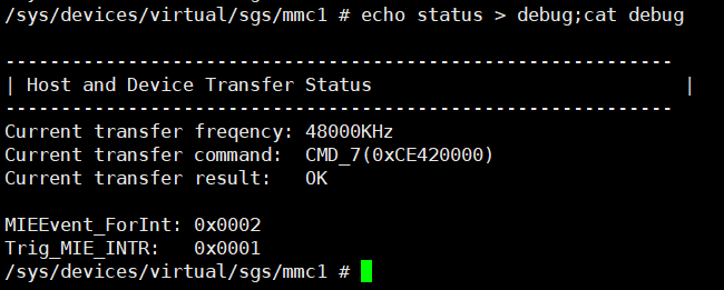
echo status > debug;cat debug
| attribute | Definition |
|---|---|
| Current transfer freqency | Displays the current operating clock frequency of the device. |
| Current transfer command | Displays the CMD and parameters of the most recent communication between the host and the device. |
| Current transfer result | Display whether the host and device's most recent communication status is normal. |
| MIEEvent_ForInt | Displays interruption information for the most recent communication record between the host and the device. |
| Trig_MIE_INTR | This displays whether the most recent communication record between the host and the device entered an interrupt service routine. 0x0001 indicates that an interrupt service routine was entered. |
MIEEvent_ForInt:
| Bit | Definition |
|---|---|
| BIT0 | Data transmission interrupted |
| BIT1 | Command transmission completed interrupted |
| BIT2 | Data transmission interrupted abnormally |
| BIT3 | SDIO D1 interrupt |
| BIT4 | Card busy end interrupt |
| BIT6 | Card insertion/removal interruption |
8.3. Read register information
echo reg > debug;cat debug
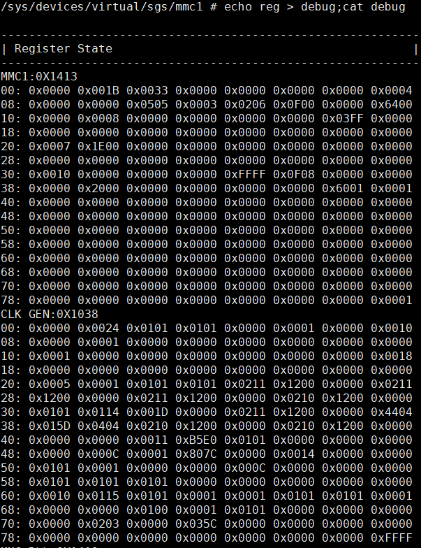
The main thing to pay attention to is the register value of offset 0xD in MMC1:0X1413, where BIT8-BIT11 represent the level state of the data line, which is high by default.
BIT0-BIT6 are error states indicated when a device malfunctions.
| Bit | Definition |
|---|---|
| BIT0 | There is a CRC checksum error when reading data. |
| BIT1 | There is a CRC checksum error when writing data. |
| BIT2 | Read/write data timeout |
| BIT3 | The host did not receive a cmd response. |
| BIT4 | The cmd response received by the host contains a CRC checksum error. |
| BIT6 | The device is in busy state |
The error code types printed in the log when an exception occurs are:
(1)SD_STS:0xFF01 Read CRC error
(2)SD_STS:0xFF02 Write CRC error
(3)SD_STS:0xFF04 Write data timeout
(4)SD_STS:0xFF08 Command sent but no response
(5)SD_STS:0xFF10 Command response has CRC error
(6)SD_STS:0xFF20 Read data timeout
(7)SD_STS:0xFF40 Device is busy
SD Card Status Register Description:
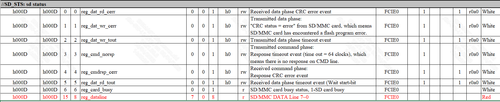
Figure 8-1: Sdmmc-14
You can find the corresponding SD card status according to the (E: 0xXXXX) information in the driver error log to determine what problem the card has.
According to the actual problems that the SD card may encounter, it is divided into the following types:
Card Recognition Failure
If the card recognition fails, it is necessary to determine whether the response acquisition fails or the transmission signal is not good and there is a CRC problem. The problem can be determined by the log printed by the driver. The specific difference and debug method are as follows:
-
SD card does not reply to command response
Phenomenon: Driver log reports (E: 0x0008) information
Debug method: First, determine whether the voltage and clock are normal. Secondly, you can capture the waveform to see whether the host has sent a command. If the first two are fine, then determine whether the card has a reply response. If there is no response, check the device status.
Related logs:
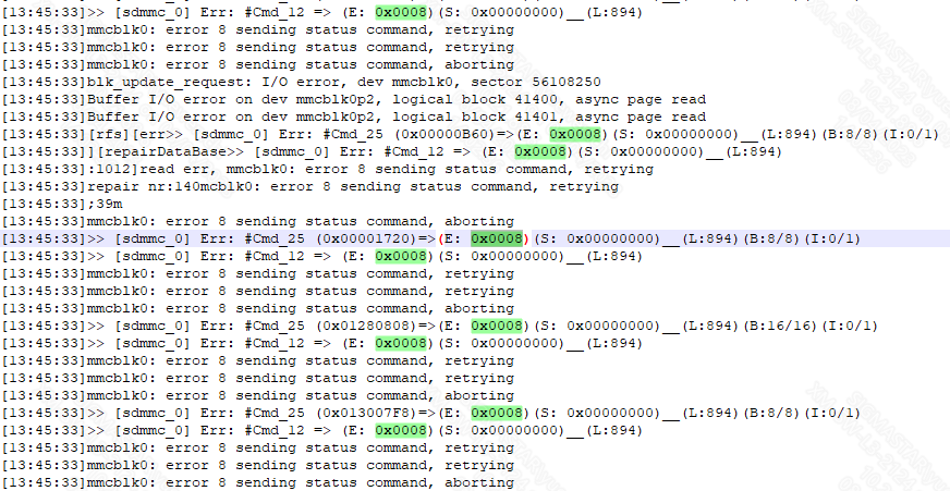
Figure 8-2: Sdmmc-15
-
Command response has CRC problem
Phenomenon: Driver log reports (E: 0x0010) information
Debug method: If there is a CRC problem, first eliminate the hardware problem, such as: whether the device contact is good, whether there is external interference, etc. Then try to change the driving gear in dts. If there is still a problem, you need to consider adjusting the clock phase.
Related logs:
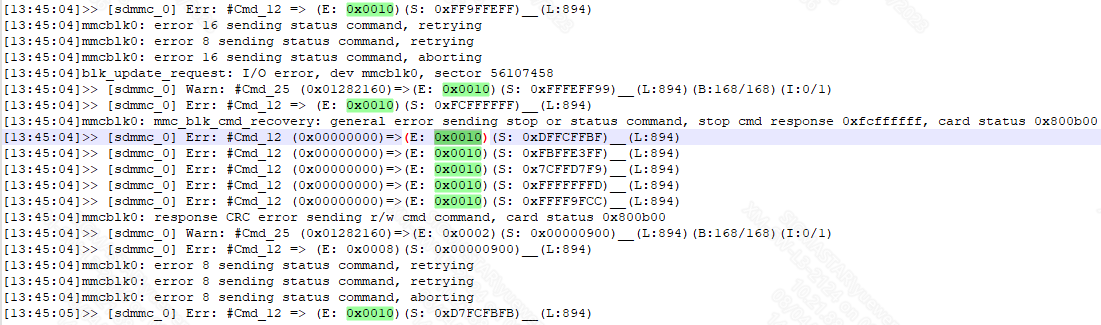
Figure 8-3: Sdmmc-16
Read and Write Failure
If you encounter a problem during normal reading and writing, you need to determine whether it is a read and write timeout problem or a CRC problem due to poor signal. You can distinguish the problem through the log. The timeout problem has the word timeout. The debug method is as follows:
-
Read and write timeout
Phenomenon: The word timeout is included in the driver error log
Debug method: First, you need to determine whether the current clock frequency and bus width are the expected configuration values. Secondly, you can increase the timeout time in the driver and try again. If there is still a timeout problem, you need to capture the waveform for detailed analysis.
The read and write timeout is set in the hal_card_platform_config.h file in the driver's corresponding chip directory:

Figure 8-4: Sdmmc-18
-
Read and write CRC problem
Phenomenon: Driver log reports (E: 0x0001) or (E: 0x0002) information
Debug method: See the previous article for debug method. In addition, for CRC problems in the read and write process, if the speed requirement is not very high, you can consider reducing the frequency or bus width.
Related logs:
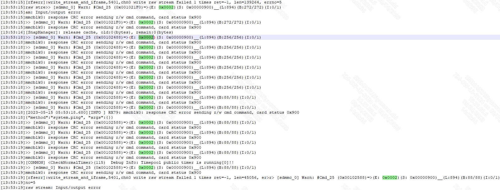
Figure 8-5: Sdmmc-17
Card Read and Write Speed Are Slow
First check whether the card clock frequency and bus width are normal. In addition, you can test and compare the read and write speeds of different models of cards.
Note: SD card reading and writing are affected by multiple factors such as the transmission time of the command and its response, the card busy time, and the stop command time. The actual read and write speeds are lower than its theoretical speed; The read and write speed test should test the read and write bandwidth of the application layer, that is, transfer a large file for testing.