SPI USER GUIDE
REVISION HISTORY
| Revision No. | Description |
Date |
|---|---|---|
| 1.0 | 04/18/2023 | |
| 1.1 | 04/08/2025 |
1. OVERVIEW
Serial Peripheral Interface (SPI), referred to as SPI, is a high-speed synchronous serial interface technology launched by Motorola. It is mainly used in EEPROM, Flash, real-time clock (RTC), analog-to-digital converter (ADC), digital signal processor (DSP) and other devices.
The brief framework of SPI driver is shown in the figure above. SGS driver registers the controller and device to SPI Core. The user APP interacts with the underlying hardware through the file interface created by SPI device to realize the read and write functions.
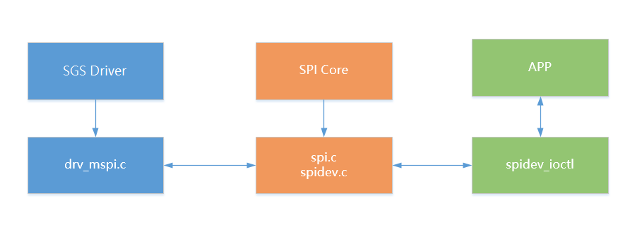
MSPI, or Master SPI device, is an IP provided by SGS specifically for use as a SPI communication master device. It can communicate with various external SPI slave devices and meet the needs of most SPI communication protocol devices.
2. KEYWORD DESCRIPTION
-
MISO / SDO: Master input slave output. (data comes from the slave)
-
MOSI / SDI: Master output slave input. (data comes from the master)
-
SCLK / SCK: Serial clock signal, generated by the master and sent to the slave.
-
CS / SS: Slave Select chip select signal, sent by the master to control which slave to communicate with, usually a low-level valid signal.
-
CPOL / CKP: Clock polarity, indicating the high and low levels of the clock in the default state.
-
CPHA / CKE: Clock phase, indicating the specific phase of the clock signal when collecting data.
-
SPI Mode: The configuration of the SPI clock polarity and phase can output 4 SPI modes.
SPI Mode CPOL CPHA 0 [00] 0 0 1 [01] 0 1 2 [10] 1 0 3 [11] 1 1
3. Functional Description
-
MSPI (Master SPI) can only be used as a master device, not a slave device.
-
The hardware supports 2 groups of MSPI and Motorola SPI standard timing. The register bank of MSPI and the maximum software chip select supported are as follows:
MSPI Bus bank addr cs_num 0 1110H 2 1 1111H 2 -
Supports full-duplex read and write, half-duplex read and write in FIFO mode, and only supports half-duplex read and write in DMA mode.
-
Supports 4-wire communication (MISO + MOSI + SCLK + CS) and 3-wire communication. (MOSI + SCLK + CS)
-
8-byte read and write buffer (FIFO mode), byte transmission 1-bit to 16-bit configurable bit width.
-
Support GPIO chip selection, which needs to be added from dtsi. For detailed methods, see 6.2.3. cs-ext section.
-
Source Clock: 12M, 104M, 108M, 144M, the actual SPI communication frequency selectable gear is 8 gears for each Source Clock division(The allocation coefficients are 2, 4, 8, 16, 32, 64, 128, 256), there are 32 gears in total, so the SPI communication frequency range is 46875K~72MHz. The target frequency can be set by assigning the max_speed_hz variable in the struct mspi_setup structure (refer to 6.3.1. User-mode reading and writing SPI section); and the actual communication frequency will select the gear closest to the target frequency but less than the target frequency. The frequency gear table is as follows.
NO. SPI Clock Rate 1 46875 2 93750 3 187500 4 375000 5 406250 6 421875 7 562500 8 750000 9 812500 10 843750 11 1125000 12 1500000 13 1625000 14 1687500 15 2250000 16 3000000 17 3250000 18 3375000 19 4500000 20 6000000 21 6500000 22 6750000 23 9000000 24 13000000 25 13500000 26 18000000 27 26000000 28 27000000 29 36000000 30 52000000 31 54000000 32 72000000 -
The number and function differences of MSPI supported by different Chips are shown in the following table
chipname mspi number auto-cs function dma nohandshake function bank iford 1 N N MSPI0: 0x1110 souffle 4 N N MSPI0: 0x1110 MSPI1: 0x1111 MSPI2:0x1112 MSPI3:0x1113 ifado 2 N N MSPI0: 0x1110 MSPI1: 0x1111 pcupid 2 N N MSPI0: 0x1110 MSPI1: 0x1119 ibopper 1 Y N MSPI0: 0x1110 ifackel 2 Y N MSPI0: 0x1110 MSPI1: 0x1111 jaguar1 4 Y Y MSPI0: 0x1110 MSPI1: 0x1111 MSPI2:0x1112 MSPI3:0x1113 ifliegen 2 Y Y MSPI0: 0x1110 MSPI1: 0x1111 ihalo 2 Y Y MSPI0: 0x1110 MSPI1: 0x1111 mhera 2 Y Y MSPI0: 0x1110 MSPI1: 0x1111
4. HARDWARE CONNECTION INTRODUCTION
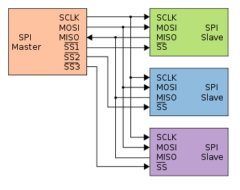
MSPI only supports one master and multiple slaves architecture. As the name implies, there can be only one master device and one or more slave devices on one bus. The slave selection signal line is often called the chip select signal line, also known as CS and SS, and is represented by SS below. When multiple SPI slave devices are connected to the SPI host, the other signal lines SCLK, MOSI and MISO of the device are connected in parallel to the same SPI bus at the same time, that is, no matter how many slave devices there are, they only use these three lines together; and each slave device has an independent SS signal line, which occupies a pin of the host, that is, there are as many chip select signal lines as there are slave devices. There is no device address in the SPI protocol. It uses the SS signal line for addressing. When the host wants to select a slave device, it sets the SS signal line of the slave device to a low level (the default is a low level), and the slave device is selected, that is, the chip select is valid, and then the host starts SPI communication with the selected slave device. Therefore, SPI communication starts with the SS line being set to a low level and ends with the SS line being pulled high.
5. UBOOT USAGE INTRODUCTION
5.1. Uboot Config Configuration
The configurations that need to be selected when compiling Uboot are as follows:
SGS drivers->

    <*> SGS MSPI->


Device drivers->

    Generic Driver Options->

        <*> Enable Driver Model

Device drivers->

    <*> SPI Support->

        <*> Enable Driver Model for SPI drivers

Command line interface->

    Device access commands->

        <*> sspi - Command to access spi device
5.2. Uboot DTS Configuration
spi0: spi0@1F222000 {
    compatible = "sgs,mspi";
    reg = <0x1F222000 0x200>;
    mspi-group = <0>;
    dma-enable;
    //nohandshake;
    cs-num = <2>;
    //cs-auto;
    cs-setup-fifo = <0>;
    cs-hold-fifo = <0>;
    cs-setup-dmatx = <0>;
    cs-hold-dmatx = <0>;
    cs-setup-dmarx = <0>;
    cs-hold-dmarx = <0>;
    //4to3-mode;
    //clk-out-mode = <27000000>;
    status = "okay";
};
| Attribute | Description | Note |
|---|---|---|
| compatible | Used to match the driver for driver registration. This attribute needs to be consistent with the code. | Modification not allowed |
| reg | Used to specify the address of SPI register bank | Modification not required |
| mspi-group | Used to specify SPI peripheral serial number | Modification not required |
| dma-enable | Used to select whether or not to enable DMA mode | Can be modified where necessary |
| nohandshake | Used to select whether or not to enable DMA nohandshake | Can be modified where necessary |
| cs-num | Used to specify the number of cs pads contained in the Engine | Used in combination with cs-ext |
| 4to3-mode | Used to select whether or not to enable 4to3 mode | Can be modified where necessary |
| clk-out-mode | Used to select whether or not to enable clk-out-mode | Can be modified where necessary |
| cs-auto | Used to select whether or not to enable hw cs mode | Can be modified where necessary |
| cs-setup-fifo | Used to change the fifo mode. The time taken to change from cs to clk in one transmission | Depend on cs-auto |
| cs-hold-fifo | Used to change the fifo mode. The time taken to change from the last clk change to the cs change in one transmission | Depend on cs-auto |
| cs-setup-dmatx | Used to change the dmatx mode. The time taken to change from cs to clk in one transmission | Depend on cs-auto |
| cs-hold-dmatx | Used to change the dmatx mode. The time taken to change from the last clk change to the cs change in one transmission | Depend on cs-auto |
| cs-setup-dmarx | Used to change the dmarx mode. The time taken to change from cs to clk in one transmission | Depend on cs-auto |
| cs-hold-dmarx | Used to change the dmarx mode. The time taken to change from the last clk change to the cs change in one transmission | Depend on cs-auto |
| status | Used to select whether or not to enable SPI master driver | Can be modified where necessary |
5.3. Uboot CMD Parameter Description and Example Screenshot
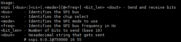
Figure 6-1: SPI-5
| Parameter | Setting Value | Description |
|---|---|---|
| 1 | sspi | Command name. |
| 2 | 0:0.1@750000 | SPI bus: CS: SPI mode: frequency. |
| 3 | 16 | The length of the data sent is 16 bits. |
| 4 | 55 | The hexadecimal data sent is 0x55. |
6. KERNEL USAGE INTRODUCTION
6.1. Kernel Config Configuration
The configurations you need to select when compiling the Kernel are as follows:
Device drivers->
    [*] SPI support->
        <*>   User mode SPI device driver support  //spidev

Device drivers->
    [*] SGS SoC platform drivers->
        <*> SGS MSPI driver
            <*> SGS SPI device driver  //SGS spidev
Note: spidev and SGS spidev are mutually exclusive. Only one can be enabled at a time. The usage differences are as follows: - spidev (
CONFIG_SPI_SPIDEV): Linux kernel standard user-mode SPI device driver. Thecompatibleof spidev sub-nodes in DTS must use standard compatibility strings (e.g.,"lwn,bk4"). This driver creates/dev/spidev<bus>.<cs>device nodes. User-space programs access SPI via standardopen/read/write/ioctl()operations on these nodes. The kernel's built-inspidev_testtool (located intools/spi/) can be used for testing. - SGS spidev (CONFIG_SGS_SPI_DEVICE): SGS proprietary SPI device driver. Thecompatibleof sub-nodes in DTS must use"sgs,mspidev". This driver does not create device nodes under/dev/. Instead, it provides a unified API viadrv_mspi.h(drv_mspi_open/read/write/transfer, etc.). This API supports both Linux (kernel-mode) and Uboot.
6.2. Dtsi Node Description
spi0: spi@1f222000{
    compatible = "sgs,mspi";
    mspi-group = <0>;
    clocks = <&CLK_mspi0>;
    reg = <0x1F222000 0x200>;
    #address-cells = <1>;
    #size-cells = <0>;
    interrupts = <GIC_SPI INT_IRQ_MSPI0 IRQ_TYPE_LEVEL_HIGH>;
    dma-enable;
    //nohandshake;
    cs-num = <2>;
    //cs-auto;
    cs-setup-fifo = <0>;
    cs-hold-fifo = <0>;
    cs-setup-dmatx = <0>;
    cs-hold-dmatx = <0>;
    cs-setup-dmarx = <0>;
    cs-hold-dmarx = <0>;
    //cs-ext = <PAD_UNKNOWN>;
    //4to3-mode;
    //clk-out-mode = <27000000>;
    status = "ok";

    spidev0@0 {
        compatible = "lwn,bk4";
        spi-max-frequency = <2000000>;
        reg = <0>;
    };

    spidev1@1 {
        compatible = "lwn,bk4";
        spi-max-frequency = <2000000>;
        reg = <1>;
    };
};
The configuration attributes supported by the SPI master driver are as follows:
| Property | Description | Remark |
|---|---|---|
| compatible | Used to match the driver for driver registration, which must be consistent with the code | Modification prohibited |
| reg | Used to specify the address of the SPI register bank | No modification required |
| interrupts | Used to specify the hardware interrupt number and attributes to be used | No modification required |
| clocks | Used to specify the clock source to use | No modification required |
| mspi-group | Used to specify the serial number of the SPI peripheral | No modification required |
| dma-enable | Used to specify whether to enable DMA mode | Can be modified as needed |
| nohandshake | Used to specify whether to enable the DMA no handshake function | Can be modified as needed |
| clk-out-mode | Used to specify whether to enable clk-out-mode | Can be modified as needed |
| cs-num | Used to specify the number of cs pads that come with the Engine | Use with cs-ext |
| cs-ext | Used to specify the pad index to be used in addition to the cs that comes with the Engine | Can be modified as needed |
| 4to3-mode | Used to specify whether to enable 4Wires to be used as 3Wires | Can be modified as needed |
| cs-auto | Used to select whether or not to enable hw cs mode | Can be modified where necessary |
| cs-setup-fifo | Used to change the fifo mode. The time taken to change from cs to clk in one transmission | Depend on cs-auto |
| cs-hold-fifo | Used to change the fifo mode. The time taken to change from the last clk change to the cs change in one transmission | Depend on cs-auto |
| cs-setup-dmatx | Used to change the dmatx mode. The time taken to change from cs to clk in one transmission | Depend on cs-auto |
| cs-hold-dmatx | Used to change the dmatx mode. The time taken to change from the last clk change to the cs change in one transmission | Depend on cs-auto |
| cs-setup-dmarx | Used to change the dmarx mode. The time taken to change from cs to clk in one transmission | Depend on cs-auto |
| cs-hold-dmarx | Used to change the dmarx mode. The time taken to change from the last clk change to the cs change in one transmission | Depend on cs-auto |
| status | Used to select whether to enable the SPI master driver | Can be modified as needed |
| spi_device | Used to register spi devices, the API using drv_mspi.h must be configured, reg indicates the chip select number | Can be increased or decreased according to demand |
| spidev | Used to register spi devices, User space exposes node /dev/spidev*.*, reg indicates the chip select number | Can be increased or decreased according to demand |
6.2.1. DMA Mode
SGS SPI Master supports two basic communication modes: fifo mode and dma mode. When the SPI Master is in fifo mode, the SPI Master driver writes the data to be sent into the SPI Master's send buffer and reads the received data from the receive buffer. The send buffer and receive buffer are registers in the SPI Master peripheral, and the capacity of the send buffer and receive buffer is 8 bytes each. Since the SPI Master works in fifo mode, the software needs to participate in the operation of the send buffer and receive buffer, so the waveform will be affected by software scheduling, and there will be a certain interval between each transmission.
When the SPI Master is in dma mode, the driver only needs to set the address of the data to be sent and the address where the received data needs to be stored to the SPI Master DMA-related registers, and the SPI Master will automatically send and receive data continuously. This process does not require software participation. Therefore, when the SPI Master works in dma mode, the SPI waveform continuity is better.
When the amount of data sent or received during the communication between the SPI Master and the SPI Device is small, you can consider using fifo mode, which has higher work efficiency. When the SPI Master and SPI Device communicate, the amount of data sent or received is large, such as receiving SPI Sensor data, etc. If fifo mode is used for such large-scale data communication, the system CPU usage will be very high, affecting system efficiency. In the scenario of large-scale data communication, dma mode can be considered.
[Note] Currently, SGS SPI Master dma mode only supports half-duplex working mode, and the sending and receiving of SPI Master share the same dma channel. When the device needs to use full-duplex communication, only fifo mode can be used. The dma-enable attribute specifies whether to use fifo mode or dma mode in half-duplex mode. When the Device driver needs to use full-duplex communication, the Master driver will automatically switch to fifo mode. When dma mode is turned on, full-duplex can be enabled through the transmission parameters, so if you want to use full-duplex mode, you can also specify the dma-enable attribute.
6.2.2. cs-num
The maximum value of the hardware preset cs number, cs-num = n, the software chip select number is the MSPI chip select 0 ~ n-1; if you want to use the MSPI software chip select cs0, cs1, you need to configure cs-num = 2.
6.2.3. cs-ext
The function of adding additional cs pins implemented by the driver. When the hardware preset cs pins are not enough, you can configure additional cs pins in dtsi as an expansion. The cs-ext chip select number starts from the value of cs-num. For example, if cs-num = 2 (indicating that hardware CS only has 2, counted as 0 and 1), the first cs-ext pin is cs2 (software-expanded CS pin, timeliness cannot be guaranteed). The method to configure additional cs is to open the cs-ext property under the dtsi node and configure the pad id to be expanded as cs. At the same time, it is recommended to configure the corresponding pad as GPIO MODE in xxx-padmux.dtsi. The following is to use PAD_I2C1_SCL as an expansion of cs:
<PAD_GPIO8         PINMUX_FOR_MSPI0_MODE_1        MDRV_PUSE_SPI0_DO>,
<PAD_GPIO9         PINMUX_FOR_MSPI0_MODE_1        MDRV_PUSE_SPI0_DI>,
<PAD_GPIO10        PINMUX_FOR_MSPI0_MODE_1        MDRV_PUSE_SPI0_CK>,
<PAD_GPIO11        PINMUX_FOR_MSPI0_MODE_1        MDRV_PUSE_SPI0_CZ>,
<PAD_I2S0_MCLK     PINMUX_FOR_MSPI0_CZ1_MODE_1    MDRV_PUSE_SPI0_CZ2>,
<PAD_I2C1_SCL      PINMUX_FOR_GPIO_MODE           MDRV_PUSE_SPI0_CZ3>,
6.2.4. clk-out-mode
clk-out-mode is a special mode supported by SGS SPI Master. When SPI Master is in clk-out-mode, MOSI and MISO of SPI Master no longer send or receive data according to the given data, and the Clock signal of SPI Master will continuously output square waves. The application scenario of this function is to use the clock output by SPI Master as the working clock of other devices. The value of clk-out-mode attribute is used to specify the frequency of the output clock. To configure clk-out-mode, you only need to turn on the clk-out-mode attribute in dtsi and configure the corresponding waveform frequency to be output:
clk-out-mode = <3750000>; //Enable clk-out-mode to output 3.75M frequency waveform
The selectable output frequency is the same as the normal operating frequency of MSPI, refer to the Frequency Range Table.
6.2.5. 4 to 3 Mode
The SPI Master 3-wire mode of some platforms does not support dma mode. If you need 3-wire dma mode communication, you can enable 4 to 3 mode. In terms of hardware, short-circuit the MOSI and MISO of the Master and connect them to the SDAT of the Device, as shown below:
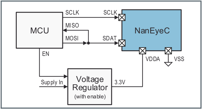
When the driver is reading data, MOSI will automatically switch to GPIO Input Mode so as not to interfere with the waveform input of MISO, thereby achieving the goal of using the four-wire mode as the three-wire mode. If you want to use this function, just turn on the 4to3-mode attribute in the dtsi node, that is
4to3-mode; // Enable 4to3-mode
Note: The pins of MSPI in 4to3 mode cannot be used as other modes. MISO in 3-wire mode can be used as other functions, provided that the mode has a higher priority than MSPI, such as gpio.
6.2.6. nohandshake
In DMA mode, the data is continuous. In the MSPI DMA module before JAGUAR1, there will be a clock delay when transferring 16Byte. Enabling this function can make up for the discontinuous DMA waveform problem.
nohandshake; // Enable DMA no handshake function
6.2.7. cs-auto
IBOPPER increases the functionality of mspi cs auto trigger, Different from the SW CS method, mspi cs auto trigger can automatically pull down the CS pin before each communication, and pull it up when staying overnight. At the same time, you can configure the time from the CS level change to the first clock level change (DTS corresponds to setup), and the time from the last clock level change to the CS level change (DTS configuration corresponds to hold)
The time consumption for phase and polarity setting in different transmission modes is as follows:
| CPHA | CPOL | cs-setup(ns) | cs-hold(ns) | cs-setup min(ns) | cs-hold min(ns) | |
|---|---|---|---|---|---|---|
| fifo | 0 | 0 | (1+k/2+n)T | (2+k+n)T | (1+k/2)T | (2+k)T |
| fifo | 0 | 1 | (1+k/2+n)T | (2+k+n)T | (1+k/2)T | (2+k)T |
| fifo | 1 | 0 | (1+n)T | (2+3k/2+n)T | T | (2+3k/2)T |
| fifo | 1 | 1 | (1+n)T | (2+3k/2+n)T | T | (2+3k/2)T |
| dmatx | 0 | 0 | k=2,(1+5k/2+n)T. k!=2,(1+k/2+n)T | (2+k+n)T | k=2,(1+5k/2)T. k!=2,(1+k/2)T | (2+k)T |
| dmatx | 0 | 1 | k=2,(1+5k/2+n)T. k!=2,(1+k/2+n)T | (2+k+n)T | k=2,(1+5k/2)T. k!=2,(1+k/2)T | (2+k)T |
| dmatx | 1 | 0 | k=2,(1+2k+n)T. k!=2,T | (2+3k/2+n)T | k=2,(1+2k)T. k!=2,T | (2+3k/2)T |
| dmatx | 1 | 1 | k=2,(1+2k+n)T. k!=2,T | (2+3k/2+n)T | k=2,(1+2k)T. k!=2,T | (2+3k/2)T |
| dmarx | 0 | 0 | (1+k/2+n)T | k=2,(2+3k+n)T. k!=2,(2+k+n)T | (1+k/2)T | k=2,(2+3k)T. k!=2,(2+k)T |
| dmarx | 0 | 1 | (1+k/2+n)T | k=2,(2+3k+n)T. k!=2,(2+k+n)T | (1+k/2)T | k=2,(2+3k)T. k!=2,(2+k)T |
| dmarx | 1 | 0 | (1+n)T | k=2,(2+7k/2+n)T. k!=2,(2+3k/2)T | T | k=2,(2+7k/2)T. k!=2,(2+3k/2)T |
| dmarx | 1 | 1 | (1+n)T | k=2,(2+7k/2+n)T. k!=2,(2+3k/2)T | T | k=2,(2+7k/2)T. k!=2,(2+3k/2)T |
The coefficient k represents the distribution coefficient of 0x49 reg_mspi_clock_rate.The values of mspi offset 0x49[10:8] are 0,1,2,3,4,5,6,7, corresponding to the distribution coefficients of 2,4,8,16,32,64,128,256.
Clock source T, if the clock source is 12M, that is, T = 1/12M = 8.3*10^-8(ns).
n is the delay register value, which is an integer (0~2^31).
When the variables of transmission configuration like cs-setup-fifo and cs-hold-fifo are less than the minimum value in the above table, the minimum value is used by default.
6.2.8. spidev
As shown in 6.2. Dts configuration above, if there is a spidev child node under the spi0 node, the reg attribute indicates the chip select number. Then when we turn on CONFIG_SPI_SPIDEV, we can see spidev0.0 (mspi0 cs0) and spidev1.0 (mspi1 cs0) in the /dev/ directory, two nodes, namely spidev<bus>.<cs>. If the sum of the chip select numbers of cs-num and cs-ext is configured to be 2, spidev0.1 (mspi0 cs1) and spidev1.1 (mspi1 cs1) will be generated.
6.3. PADMUX Configuration
The padmux configuration method of MSPI in Uboot and Kernel environments is the same. You only need to add the following code to the corresponding padmux.dtsi according to the selected pins. Taking MSPI0 as an example, each PADMUX mode requires the configuration of 4 pins:
// MSPI0 MODE 1
<PAD_GPIO8   PINMUX_FOR_MSPI0_MODE_1 MDRV_PUSE_SPI0_DO>,
<PAD_GPIO9   PINMUX_FOR_MSPI0_MODE_1 MDRV_PUSE_SPI0_DI>,
<PAD_GPIO10  PINMUX_FOR_MSPI0_MODE_1 MDRV_PUSE_SPI0_CK>,
<PAD_GPIO11  PINMUX_FOR_MSPI0_MODE_1 MDRV_PUSE_SPI0_CZ>,

// MSPI1 MODE 1
<PAD_GPIO12   PINMUX_FOR_MSPI1_MODE_1 MDRV_PUSE_SPI1_DO>,
<PAD_GPIO13   PINMUX_FOR_MSPI1_MODE_1 MDRV_PUSE_SPI1_DI>,
<PAD_GPIO14   PINMUX_FOR_MSPI1_MODE_1 MDRV_PUSE_SPI1_CK>,
<PAD_GPIO15   PINMUX_FOR_MSPI1_MODE_1 MDRV_PUSE_SPI1_CZ>,
Parameter description:
The first column is the pin index number, which can be found in drivers/sgs_common/gpio/hal/{chipname}/pub/gpio.h;

The second column is the mode definition. In the m_hal_gpio_st_padmux_entry array in drivers/sgs_common/gpio/hal/{chipname}/src/hal_pinmux.c, the multiplexing relationship of all pins is listed. To query which multiplexing functions the pin supports, you can query the array;

The third column is the index name of the pin and the matching mode, which can be queried in drivers/sgs_common/padmux/hal/{chipname}/pub/drv_puse.h.
6.4. Module usage introduction
The kernel comes with a set of Device Driver and user programs for testing MSPI Master: drivers/spi/spidev.c and tools/spi/spidev_test.c.
6.4.1. Read and write SPI in user mode
-
To use the kernel's built-in test program spidev_test.c, you need to modify the configuration file to open the CONFIG_SPI_SPIDEV option and configure the spidev subnode in dts. The kernel will eventually generate spidevX.X files in the /dev folder.
-
User-mode test case, execute make in the tools/spi/ directory to obtain the executable file spidev_test.
Common operations of spidev_test are:
Parameter Description -D Used to select the device node for the operation, such as: /dev/spidev0.0, the default is: /dev/spidev1.1. -s Used to select the spi clock rate, the unit is Hz. -H Used with -O to select the spi communication timing. -O Used with -H to select the spi communication timing. -C Used to specify that CS is active high. -L Used to specify the byte order as LSB. -3 Used to specify the communication mode as 3-wire mode. -v Used to specify the printed data content to be sent & received. -i Used to specify the file to be sent. (binary file) -o Used to specify the path to save the received data into a file. (binary file) -p Used to specify the data to be sent, such as: "1234\xde\xad". The functions supported by the current driver are listed in the table above. For specific usage, please refer to the help command:
spidev_test help. Parameters can be combined freely, please adjust as needed. -
The spidev_test core send/receive function example is as follows:
static void transfer(int fd, uint8_t const *tx, uint8_t const *rx, size_t len) { int ret; int out_fd; struct spi_ioc_transfer tr = { .tx_buf = (unsigned long)tx, .rx_buf = (unsigned long)rx, .len = len, .delay_usecs = delay, .speed_hz = speed, .bits_per_word = bits, }; if (mode & SPI_TX_OCTAL) tr.tx_nbits = 8; else if (mode & SPI_TX_QUAD) tr.tx_nbits = 4; else if (mode & SPI_TX_DUAL) tr.tx_nbits = 2; if (mode & SPI_RX_OCTAL) tr.rx_nbits = 8; else if (mode & SPI_RX_QUAD) tr.rx_nbits = 4; else if (mode & SPI_RX_DUAL) tr.rx_nbits = 2; if (!(mode & SPI_LOOP)) { if (mode & (SPI_TX_OCTAL | SPI_TX_QUAD | SPI_TX_DUAL)) tr.rx_buf = 0; else if (mode & (SPI_RX_OCTAL | SPI_RX_QUAD | SPI_RX_DUAL)) tr.tx_buf = 0; } ret = ioctl(fd, SPI_IOC_MESSAGE(1), &tr); if (ret < 1) pabort("can't send spi message"); if (verbose) hex_dump(tx, len, 32, "TX"); if (output_file) { out_fd = open(output_file, O_WRONLY | O_CREAT | O_TRUNC, 0666); if (out_fd < 0) pabort("could not open output file"); ret = write(out_fd, rx, len); if (ret != len) pabort("not all bytes written to output file"); close(out_fd); } if (verbose) hex_dump(rx, len, 32, "RX"); } -
When .rx_buff is not null and .tx_buff is null in struct spi_ioc_transfer tr, MSPI Master performs half-duplex read operation; when .rx_buff is null and .tx_buff is not null, half-duplex write operation is performed; when .rx_buff and .tx_buff are not null, even if dma mode is turned on, full-duplex read and write operation of fifo mode is performed. The corresponding waveform diagram is as follows:
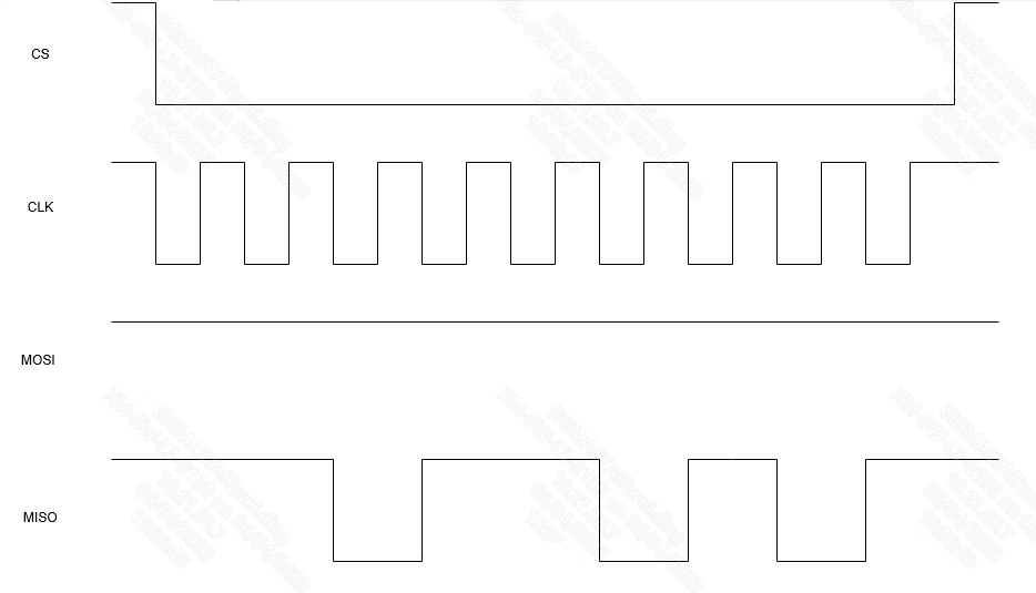
Figure 7-2: Waveform DiagramIn the figure, MOSI corresponds to the data in .tx_buff, and MISO corresponds to the data in .rx_buff.
6.4.2. Read and write SPI in kernel mode
For kernel-mode reading and writing of MSPI, refer to the implementation of /drivers/spi/spidev.c, encapsulate the interface to build and initialize the structures spi_transfer and spi_message, and then call the kernel interface spidev_sync():
spidev_sync_read(struct spidev_data *spidev, size_t len)
{
    struct spi_transfer t = {
            .rx_buf     = spidev->rx_buffer,
            .len        = len,
            .speed_hz   = spidev->speed_hz,
        };
    struct spi_message  m;

    spi_message_init(&m);
    spi_message_add_tail(&t, &m);
    return spidev_sync(spidev, &m);
}

spidev_sync_write(struct spidev_data *spidev, size_t len)
{
    struct spi_transfer t = {
            .tx_buf     = spidev->tx_buffer,
            .len        = len,
            .speed_hz   = spidev->speed_hz,
        };
    struct spi_message  m;

    spi_message_init(&m);
    spi_message_add_tail(&t, &m);
    return spidev_sync(spidev, &m);
}
7. API Reference
Linux header file path: drivers/sgs_common/include/drv_mspi.h
Linux demo path: drivers/sgs_common/mspi/drv/src/drv_spidev_test_lnx.c
This function module provides the following interfaces:
| API | Function |
|---|---|
| drv_mspi_open | Create a device handle |
| drv_mspi_rel | Destroy the device handle |
| drv_mspi_set | Setting Hardware Parameters |
| drv_mspi_write | MSPI only sends data (half-duplex) |
| drv_mspi_read | MSPI only receives data (half-duplex) |
| drv_mspi_transfer | MSPI reads and writes data simultaneously (full-duplex) |
7.1. drv_mspi_open
-
Function
Create a device handle.
-
Grammar
int drv_mspi_open(mspi_handle *handle, u32 nr);
-
Parameter
Parameter name Description Input/Output handle Device Information Output nr Bus number Input -
Return Value
Return value Description 0 Success other Failure
7.2. drv_mspi_rel
-
Function
Destroys the device handle.
-
Grammar
int drv_mspi_rel(mspi_handle *handle);
-
Parameter
Parameter name Description Input/Output handle Device Information Input -
Return Value
Return value Description 0 Success other Failure -
Notice
handle is the reverse operation of open and needs to be called after using open.
7.3. drv_mspi_set
-
Function
Set the hardware parameters.
-
Grammar
int drv_mspi_set(mspi_handle *handle, mspidev_cfg *cfg);
-
Parameter
Parameter name Description Input/Output handle Device Information Input cfg Transport Configuration Parameters Input -
Return Value
Return value Description 0 Success other Failure -
Notice
The handle must be created by open.
7.4. drv_mspi_write
-
Function
Send data.
-
Grammar
int drv_mspi_write(mspi_handle *handle, u8 *buf, u32 count);
-
Parameter
Parameter name Description Input/Output handle Device Information Input buf Data to send Input count Data length (Byte) Input -
Return Value
Return value Description 0 Success other Failure -
Notice
The handle must be created by open. Before calling, you need to set the hardware parameters with drv_mspi_set.
7.5. drv_mspi_read
-
Function
Get data.
-
Grammar
int drv_mspi_read(mspi_handle *handle, u8 *buf, u32 count);
-
Parameter
Parameter name Description Input/Output handle Device Information Input buf Received data Input count Data length (Byte) Input -
Return Value
Return value Description 0 Success other Failure -
Notice
The handle must be created by open. Before calling, you need to set the hardware parameters with drv_mspi_set.
7.6. drv_mspi_transfer
-
Function
Read and write data.
-
Grammar
int drv_mspi_transfer(mspi_handle *handle, mspi_tfr *xfer, u32 n_xfers);
-
Parameter
Parameter name Description Input/Output handle Device Information Input xfer Transfer data structure Input n_xfers Number of xfers Input -
Return Value
Return value Description 0 Success other Failure -
Notice
The handle must be created by open. Before calling, you need to set the hardware parameters with drv_mspi_set.
8. FAQ
8.1 SPI communication cannot capture waveform
-
Check whether the driver is loaded normally and whether there is an error during the startup process.
-
Check whether the padmux configuration is correct.
-
Check whether the hardware circuit is abnormal, configure the pin to GPIO output mode, and use a voltmeter to measure whether the GPIO high and low levels can jump normally.
8.2 SPI cannot read device data
-
Check whether the clock rate configured by mspi is greater than the maximum clock supported by the peripheral.
-
Check whether the data pin is connected incorrectly, DO of MSPI is MISO, and DI is MOSI.
-
Capture the sent waveform to see if it meets the waveform required by the peripheral.
-
Is the peripheral normal.
8.3 The waveform is messy
-
Check whether the voltage matches
-
The pin drive capability may be insufficient, increase the pin drive capability.