Adc_DebugSop
REVISION HISTORY
| Revision No. | Description |
Date |
|---|---|---|
| 1.0 | 07/18/2025 |
1. Debug Flow Chart
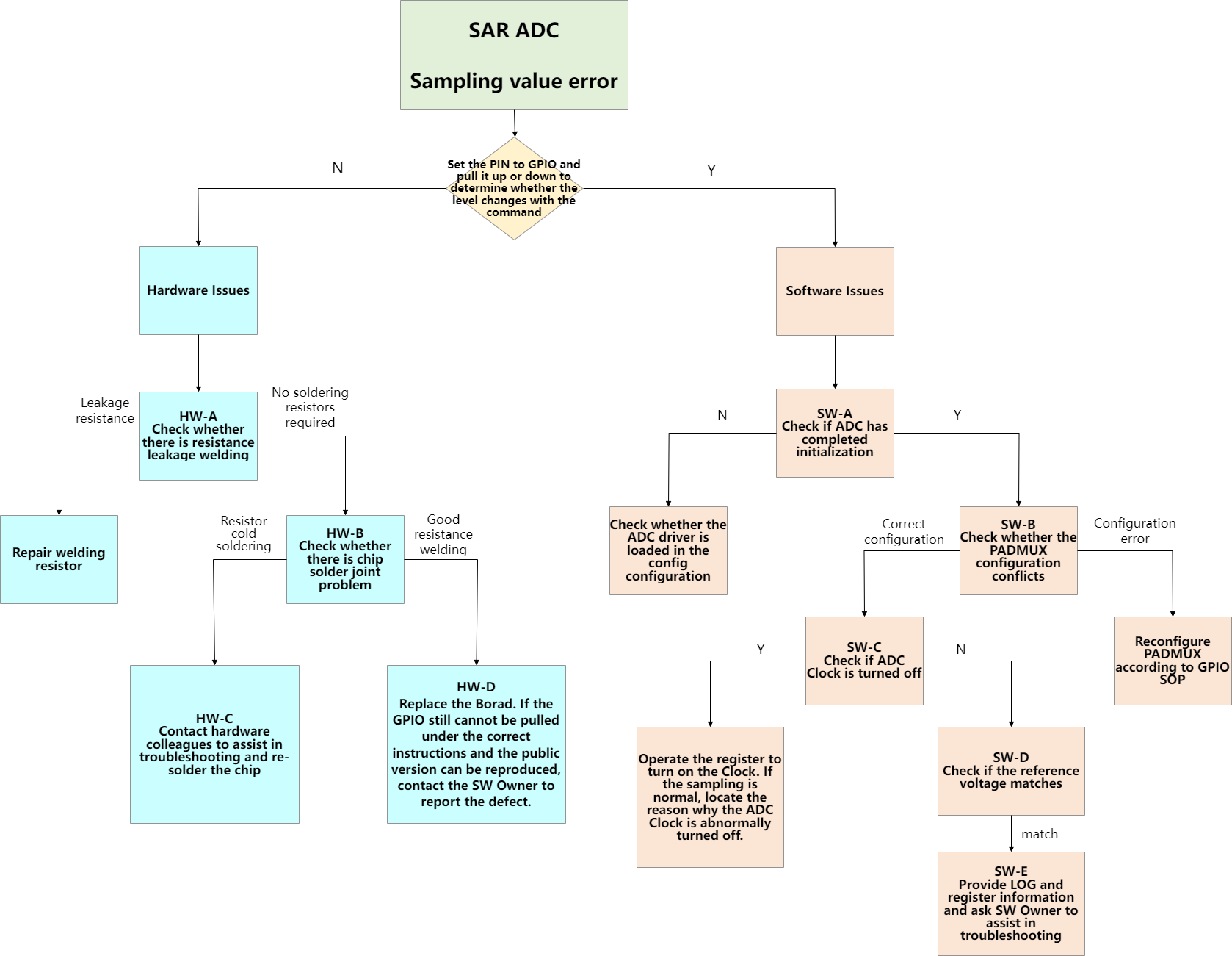
2. Explanation of the Debug Flow
2.1 Hardware Issues
When incorrect ADC sampling values are detected, you can manipulate registers or use GPIO commands to set the corresponding PIN to GPIO and toggle it high and low (note that some PINs may not have GPIO functionality as the highest priority, in which case you need to clear higher priority settings first), how to operate:
riu_w 0x14 0x11 0x00  //set GPIO MODE
riu_w 0x14 0x12 0xff  //set high level
riu_w 0x14 0x12 0x00  //set low level
If the actual output level does not change, it can be determined to be a hardware issue, and you can troubleshoot in the following order:
2.1.1 HW-A Check Resistors And Traces
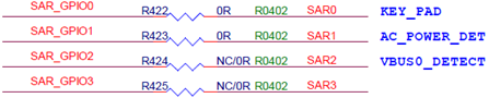
Check whether there is any resistor leakage on the corresponding PIN pin of the schematic diagram. As shown in the figure below, R424 and R425 need to be connected to a 0R resistor.
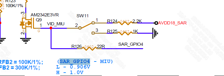
Check whether the corresponding PIN pin routing in the schematic diagram is grounded. As shown in the figure below, if the jumper cap of SW11 is connected to 2-3, SAR_GPIO4 is grounded and the ADC sampling value cannot be obtained.
2.1.2 HW-B Check Soldering Conditions
If the GPIO can toggle high and low after changing the Board, it may indicate a cold solder joint on the chip, requiring rework.
2.1.3 HW-C Request Assistance
Contact hardware colleagues for assistance in troubleshooting and re-soldering the chip.
2.1.4 HW-D Issue Reporting
If the GPIO still cannot toggle high and low after changing the Board, please contact FAE to report the issue.
2.2 Software Issues
If it is a software problem, you can troubleshoot in the following order:
2.2.1 SW-A Check ADC initialization status
Check whether ADC has completed initialization through the configuration of Bank 0x14, mainly check whether the value of 0x0 is 0xA20, and whether there are values in 0x40~0x47:
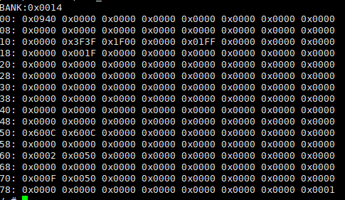
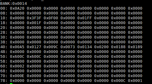
If initialization is not completed, sampling is naturally impossible. Please check whether the SAR ADC driver is loaded in the config configuration.
Linux config:
Device Drivers --->
[*] Sgs SoC platform drivers --->

    <*> Sgs ADC driver

        <*> Sgs ADCLP driver
Linux DTS:
adclp0: adclp0@1f002800 {    // Select channel 0
    compatible = "sgs,adclp";
    ......
    status = "ok";  // Ok:Initialize ADC
};
Rtos config:
BSP Driver Options --->

    <*> Support SARADC driver
Rtos Sysdesc:
<adclp0>     // Select channel 0
    [reg_u32] 0x1F002800;
    ......
    [status_u8] 1; // 1:Initialize ADC
2.2.2 SW-B Check PADMUX
After ADC is initialized, if the voltage value still cannot be obtained correctly, you need to check whether there is a conflict in PADMUX. For details, see the PADMUX conflict check content in Gpio_DebugSop. Generally, the ADC pin cannot be sampled after being set to GPIO MODE. You can directly read the value of 0x14 0x11 BIT0~BIT5 to judge. Each BIT corresponds to a channel one by one.
riu_r 0x14 0x11 -> 0x3E3E  //adc channel0 is set to GPIO MODE
riu_r 0x14 0x11 -> 0x3F3F  //adc channel0 is set to ADC MODE
2.2.3 SW-C Check CLK Source
Check the following registers to confirm whether the ADC clock source is turned off:
0xE 0x22 BIT5
If BIT5 = 0, it means the ADC clock source is turned on. If BIT5 = 1, it means the ADC clock source is abnormally turned off. Please contact SW Owner debugger.
2.2.4 SW-D Check Reference Voltage
Check the following registers to confirm the reference voltage level of each ADC channel:
0x14 0x19 BIT0 corresponds to channel 0, BIT1 corresponds to channel 1, and so on
When the BIT value is 1, the reference voltage of the channel is 1.8V, and when the BIT value is 0, the reference voltage of the channel is 1.0V. (The reference voltage corresponding to BIT 1/0 of some chips is 3.3V/2.0V). Please confirm whether an unmatched reference voltage is used when calculating the voltage.
2.2.5 SW-E Request Assistance
If all the above steps are checked and OK, please provide ADC-related LOG and ADC configuration information , and contact FAE for debugging assistance.
3. Common questions
3.1. Abnormal ADC sampling value
No matter how the external input voltage is adjusted, the ADC value of a certain channel is abnormal. Please refer to 2.2.2 SW-B Check PADMUX to determine whether this channel is switched to GPIO MODE
3.2. ADC sampling value gradually increases or decreases, and stabilizes after a period of time
When the external input voltage is stable: if the PIN pin is switched back from GPIO MODE to ADC MODE, the PIN pin needs a certain amount of time to reach a steady state. At this time, it is not recommended to obtain the ADC value immediately after switching.
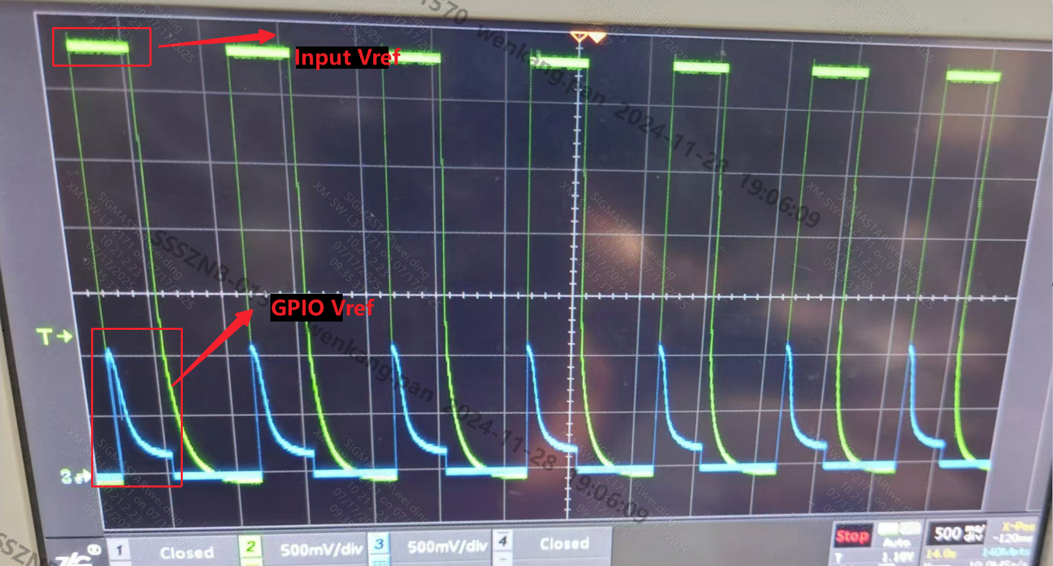
When the external voltage is unstable: At this time, the sampling point is most likely during the rising or falling edge. You can use the GPIO operation to confirm during sampling. As shown in the following figure, when the ADC is sampling, set another PIN to GPIO and pull it low. You can see that the sampling timing falls on the falling edge.